What Is Graphene?
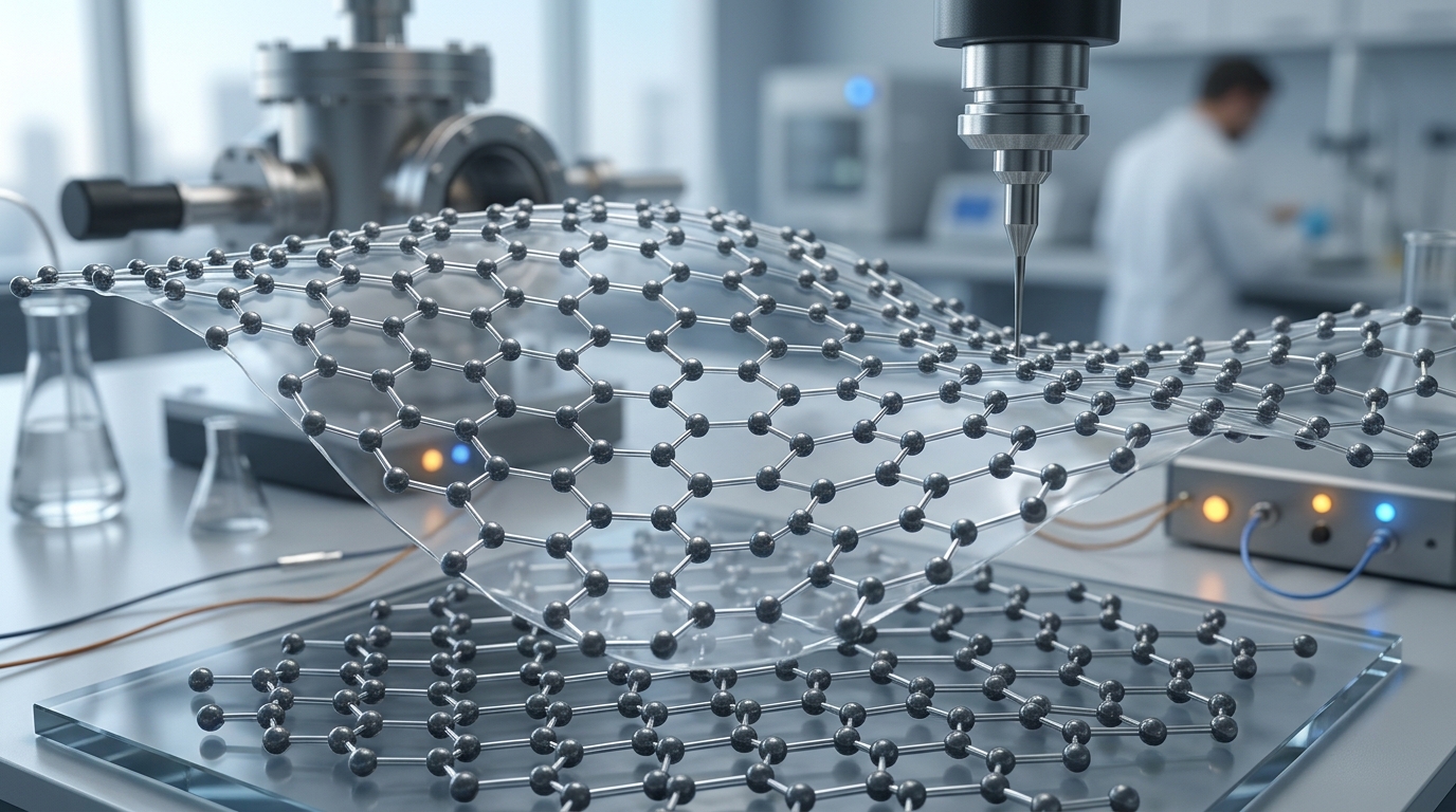
Graphene is a single layer of carbon atoms tightly arranged in a two-dimensional hexagonal honeycomb lattice. It is the foundational structural element of several other carbon allotropes, including graphite, carbon nanotubes, and fullerenes. Despite measuring only one atom in thickness—roughly 0.34 nanometers—graphene is one of the strongest, lightest, and most conductive materials known to modern science.
The Core Definition and Structure of Graphene
At an atomic level, graphene consists entirely of carbon atoms bound together through sp2 hybridization. In this configuration, each carbon atom shares strong covalent bonds with three adjacent neighbors in a planar sheet. The fourth valence electron occupies a vertical p-orbital, which delocalizes across the entire sheet to form overlapping pi bands. This delocalized electronic network gives graphene its extraordinary electrical and thermal conductivity.
Because it comprises a single atomic layer, graphene is classified as a two-dimensional (2D) material. Prior to its physical isolation, theoretical physicists debated whether purely two-dimensional crystal lattices could remain thermodynamically stable at room temperature without curling, folding, or decomposing.
Discovery and the Nobel Prize in Physics
Carbon layers resembling graphene were observed in transmission electron microscopes for decades, but isolating a freestanding, single-atom-thick sheet remained elusive until 2004. Researchers Andre Geim and Konstantin Novoselov at the University of Manchester succeeded in isolating single-layer graphene using a surprisingly straightforward technique: mechanical exfoliation.
By pressing standard adhesive tape against high-purity graphite and repeatedly peeling it apart, they systematically separated the weakly bound graphite layers until single-atom sheets remained. They transferred these flakes onto a silicon dioxide substrate, confirming their monolayer structure under optical and atomic force microscopy. This breakthrough unlocked a wave of solid-state physics research and earned Geim and Novoselov the 2010 Nobel Prize in Physics.
Key Physical and Chemical Properties
Graphene combines mechanical, thermal, electrical, and optical properties rarely found together in a single substance:
- Exceptional Mechanical Strength: Monolayer graphene boasts an intrinsic tensile strength of approximately 130 gigapascals (GPa) and a Young’s modulus of roughly 1 terapascal (TPa). On an equivalent mass-to-mass basis, it is over 100 times stronger than structural steel while remaining exceptionally flexible.
- High Electrical Conductivity and Electron Mobility: In pristine graphene, charge carriers (electrons and holes) behave as massless Dirac fermions. This allows room-temperature electron mobility exceeding 15,000 to 200,000 cm2/(V·s) in suspended or clean substrate environments, enabling ultra-fast charge transfer with minimal resistance.
- Superior Thermal Conductivity: Graphene exhibits ballistic thermal transport at room temperature, with thermal conductivity values typically measured between 3,000 and 5,000 W/(m·K). This substantially outperforms conventional thermal conductors like copper and silver.
- Optical Transparency: Despite being dense enough to block the smallest gas atoms (such as helium), a single layer of graphene absorbs only about 2.3% of incident white light, making it roughly 97.7% transparent to the naked eye.
- Impermeability: The overlapping electron clouds within the hexagonal carbon rings create an energy barrier that prevents atoms and molecules from passing through the pristine lattice under standard conditions.
Graphene Compared to Other Carbon Allotropes
Carbon possesses a unique ability to form diverse allotropes depending on its bonding geometry and dimensional structure. Understanding how graphene relates to other allotropes clarifies its structural role:
| Allotrope | Dimensionality | Bonding | Key Structural Feature |
|---|---|---|---|
| Graphene | 2D (Planar sheet) | sp2 | Single atomic layer in a hexagonal lattice. |
| Graphite | 3D (Bulk crystal) | sp2 (in-plane) | Millions of stacked graphene sheets held together by weak van der Waals forces. |
| Diamond | 3D (Tetrahedral crystal) | sp3 | Rigid 3D lattice; electrically insulating, ultra-hard, and optically transparent. |
| Carbon Nanotubes (CNTs) | 1D (Tubular cylinder) | sp2 | A graphene sheet rolled seamlessly into a single-walled or multi-walled tube. |
| Fullerenes (Buckyballs) | 0D (Spherical cage) | sp2 | Graphene-like hexagonal rings mixed with pentagonal rings folded into a sphere. |
Common Commercial Forms of Graphene Materials
In research and commercial supply chains, the term “graphene” frequently encompasses several distinct material grades. Each grade features different properties, processing characteristics, and cost profiles:
1. Monolayer and Few-Layer Graphene (FLG)
Monolayer graphene consists of a single isolated sheet. Few-layer graphene typically ranges from 2 to 10 stacked layers. These forms preserve most of the pristine electrical and mechanical properties of the 2D lattice and are primarily used in high-performance electronics, optoelectronics, and precision sensors.
2. Graphene Nanoplatelets (GNPs)
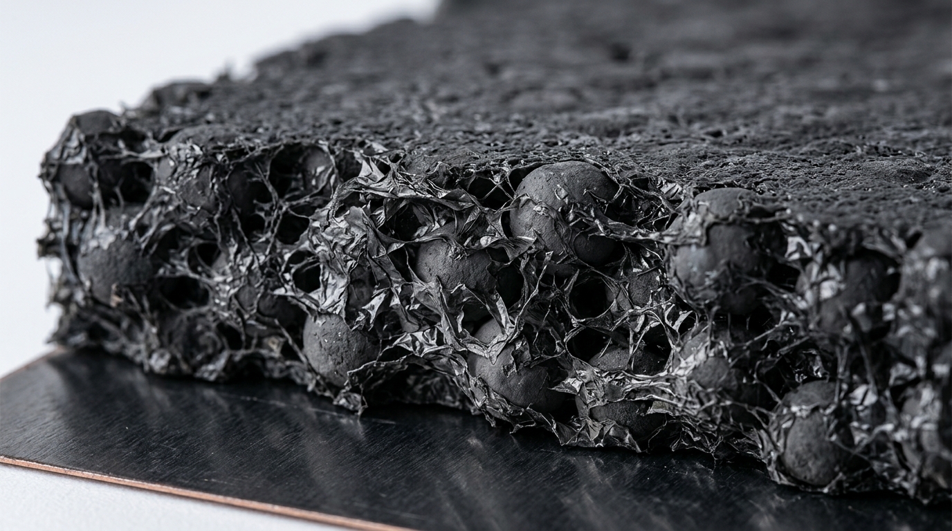
Graphene nanoplatelets consist of small stacks of graphene sheets ranging from 10 to over 50 layers, with thicknesses between 2 and 100 nanometers. While they lack the pristine quantum electronic behavior of single sheets, they provide substantial mechanical reinforcement, thermal conduction, and electrical conductivity when dispersed as additives in polymers, lubricants, and building materials.
3. Graphene Oxide (GO)
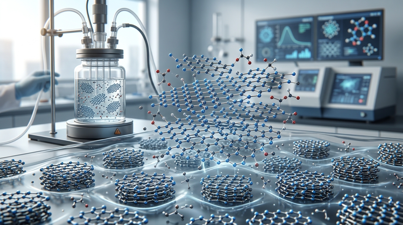
Graphene oxide is produced by treating graphite with strong oxidizing agents. This chemical exfoliation introduces oxygen-containing functional groups—such as hydroxyl, epoxy, and carboxyl groups—onto the basal planes and edges. Graphene oxide is electrically insulating and chemically reactive, but its hydrophilicity allows it to disperse readily in water and organic solvents, making it a versatile precursor for coatings, films, and membranes.
4. Reduced Graphene Oxide (rGO)
When graphene oxide undergoes thermal, chemical, or electrochemical reduction to remove oxygen groups, it becomes reduced graphene oxide. Although structural defects remain from the oxidation process, rGO partially restores electrical conductivity and provides a scalable, cost-effective route for energy storage electrodes and conductive inks.
Primary Synthesis and Production Methods
The manufacturing process determines the defect density, flake size, layer count, and economic viability of graphene:
- Mechanical Exfoliation (Scotch-Tape Method): Uses adhesive forces to peel pristine flakes from bulk graphite. This method produces the highest quality crystals for fundamental physics experiments, but yields are minute and unsuited for industrial manufacturing.
- Chemical Vapor Deposition (CVD): Involves decomposing hydrocarbon gases (such as methane) at elevated temperatures over metallic catalytic substrates, typically copper or nickel foils. CVD produces large-area, high-uniformity single-layer films required for semiconductor devices, flexible touch displays, and transparent conductive electrodes.
- Liquid-Phase Exfoliation (LPE): Uses ultrasonic energy, high-shear mixing, or microfluidization to break apart graphite in liquid media or surfactant solutions. LPE delivers high volumes of few-layer graphene flakes and nanoplatelets suitable for bulk additives, inks, and conductive coatings.
- Oxidation-Reduction (Hummer’s Method): Graphite is chemically oxidized to graphene oxide, exfoliated in solution, and subsequently reduced. This process supports mass manufacturing of powder and slurry forms for energy storage and composite reinforcement.
Major Application Domains
Graphene’s diverse properties support practical applications across multiple scientific and industrial sectors:
Electronics and Photonics
Because of its electron mobility and atomic thinness, graphene is studied for high-frequency transistors, photodetectors, transparent electrodes for flexible displays, and heat spreaders in microprocessors. However, pristine graphene lacks a natural electronic bandgap, meaning it cannot be switched off completely like silicon. As a result, pure graphene is often combined with other semiconductors or used in specialized radio-frequency and analog circuits rather than standard digital logic switches.
Energy Storage and Conversion
Adding graphene, GO, or rGO to battery electrodes enhances electrical transport, facilitates faster ion diffusion, and reduces thermal degradation. In lithium-ion batteries and supercapacitors, graphene-enhanced anodes and cathodes support faster charging rates, higher power densities, and improved cycle lifetimes.
Advanced Composites and Structural Materials
Integrating graphene nanoplatelets into polymers, metals, and concrete improves mechanical strength, lowers weight, and imparts anti-corrosion properties. In civil engineering, small weight percentages of graphene dispersed in concrete matrices accelerate curing, improve compressive strength, and decrease permeability against moisture and chemical degradation.
Water Purification and Membrane Separation
Graphene oxide laminates and nanoporous graphene sheets feature tunable nanochannels that allow water molecules to pass rapidly while blocking dissolved ions, organic pollutants, and heavy metals. These engineered membranes offer potential efficiency gains for industrial desalination, water recycling, and selective gas separation.
Biomedical Technologies
Functionalized graphene materials are actively researched for targeted drug delivery carriers, biosensors, and tissue engineering scaffolds. Graphene-based field-effect biosensors can detect minute concentrations of biomolecules, pathogens, or viral proteins by registering changes in electrical conductivity upon surface binding.
Commercial Reality vs. Common Misconceptions
While graphene is often celebrated as a transformative material, practical industrial adoption requires addressing key manufacturing and economic challenges:
- The Scalability Gap: Laboratory-synthesized graphene produced via CVD exhibits near-theoretical properties, but scaling that quality to continuous roll-to-roll manufacturing without defects or contamination remains technically demanding and costly.
- Nomenclature Precision: Many commercial “graphene” products contain multi-layer graphene nanoplatelets or modified graphite rather than true single-layer graphene. Standardized terminology set by organizations like ISO ensures clarity regarding layer count and chemical purity.
- Dispersion and Agglomeration: In composite manufacturing, graphene flakes tend to re-stack due to strong inter-sheet van der Waals forces. Specialized surface functionalization, surfactants, and shear-mixing techniques are required to maintain uniform dispersion inside host matrices.
As synthesis techniques mature and international material standards take hold, graphene continues to transition from an experimental discovery into a practical additive and platform material across global industries.