
Graphene Market
The global graphene market does not revolve around a single, uniform commodity. Instead, it encompasses a diverse ecosystem of carbon-based nanomaterials tailored for specific industrial demands. From high-volume powders reinforcing structural polymers to pristine monolayer films integrated into high-speed photodetectors, commercial viability depends on matching the correct material morphology to the right industrial application. Understanding this market requires examining production methods, cost dynamics, performance trade-offs, and the physical engineering challenges of moving from laboratory synthesis to scaled manufacturing.
Material Segmentation: The Core Commercial Forms
Graphene materials are broadly segmented into two primary categories: bulk graphene powders and continuous thin films. These two categories differ substantially in their synthesis mechanisms, cost structures, physical properties, and target applications.
Bulk Graphene: Platelets, Oxides, and Slurries
Bulk forms represent the largest share of physical volume in the market. These materials are produced via top-down exfoliation of graphite or bottom-up combustion synthesis, typically sold as dry powders, aqueous pastes, or liquid masterbatches.
- Graphene Nanoplatelets (GNPs): Multilayer stacks ranging from a few layers up to dozens of layers of graphene sheets. GNPs offer high electrical conductivity, mechanical stiffness, and thermal dissipation at a relatively accessible cost profile. They serve primarily as functional additives in polymers, elastomers, and concrete.
- Graphene Oxide (GO): Heavily oxygenated flakes produced through chemical oxidation. GO is water-dispersible and chemically reactive, making it suitable for water filtration membranes, biomedical scaffolds, and chemical sensors. However, the oxidation process disrupts the sp2 carbon lattice, making GO electrically insulating.
- Reduced Graphene Oxide (rGO): Created by chemically, thermally, or electrochemically removing oxygen functional groups from GO. While rGO restores a significant portion of electrical and thermal conductivity, residual structural defects keep its performance below pristine graphene. It is widely used in conductive coatings and energy storage electrodes.
Continuous Films: CVD and Epitaxial Graphene
Continuous thin films target high-value, lower-volume technical applications. These sheets are synthesized via bottom-up methods such as chemical vapor deposition (CVD) on catalytic metallic substrates like copper or nickel, or through high-temperature sublimation on silicon carbide (SiC).
Monolayer CVD films retain the exceptional electron mobility and optical transparency associated with ideal graphene. These films are utilized in transparent conducting electrodes, broadband photodetectors, Hall effect sensors, and high-frequency analog devices. The primary limitation of continuous films lies in the cost, throughput, and defect generation associated with transferring the atomic layer from the metal foil to target substrates such as silicon or flexible polymers.
| Material Form | Primary Synthesis Route | Key Properties | Primary Industrial Uses |
|---|---|---|---|
| Graphene Nanoplatelets (GNP) | Liquid-phase or mechanical exfoliation | High aspect ratio, mechanical stiffness, thermal conductivity | Automotive plastics, anti-corrosion primers, thermal interface pads |
| Graphene Oxide (GO) | Modified Hummers’ method (chemical oxidation) | High hydrophilicity, processable in water, insulating | Separation membranes, environmental remediation, biochemical assays |
| Reduced Graphene Oxide (rGO) | Thermal or chemical reduction of GO | Moderate electrical conductivity, porous network formation | Battery anodes, supercapacitors, conductive inks |
| Monolayer CVD Films | Catalytic methane pyrolysis on metal foil | Ultra-high carrier mobility, 97.7% optical transparency | Optical modulators, magnetic sensors, advanced semiconductor logic |
Supply Chain Mechanics and Production Economics
The pricing and availability of graphene depend heavily on feedstock sourcing, energy inputs, and quality assurance protocols. Unlike base metals, graphene lacks a unified spot market price because value correlates strictly with flake dimensions, layer count, surface functionality, and purity.
Raw Material Feedstocks
For bulk graphene, the primary starting material is natural flake graphite or synthetic graphite. The market is therefore linked to the broader graphite extraction and refining sector. Chemical processing methods require access to bulk mineral acids, oxidizing agents, and neutralization chemicals. Bottom-up powder processes utilize hydrocarbon gases, biomass waste, or liquid alcohols via plasma torches and detonation chambers, bypassing graphite mining entirely.
For CVD graphene, the primary feedstocks are high-purity hydrocarbon gases (such as methane and ethylene), carrier gases (hydrogen and argon), and high-grade copper or nickel foils. Substrate preparation and post-growth transfer consumables constitute a major portion of production expenditure.
The Cost-to-Performance Equation
In industrial manufacturing, graphene must justify its integration against incumbent additives such as carbon black, carbon fibers, synthetic graphite, and carbon nanotubes (CNTs). While graphene often provides superior specific surface area and electrical performance, end users evaluate material cost based on the total loading percentage required to achieve a target specification.
For example, if adding 0.5% by weight of high-grade GNPs achieves the same electrical percolation threshold as 10% conventional carbon black, the reduced mass, preserved mechanical properties of the base polymer, and improved processing rheology can justify the higher per-kilogram price of the nanomaterial.
Key Demand Sectors Driving Commercial Adoption
The industrial uptake of graphene follows distinct timelines depending on qualification cycles, regulatory demands, and processing compatibility across several major industries.
1. Energy Storage and Batteries
Graphene serves as a functional additive in both the anode and cathode assemblies of lithium-ion, sodium-ion, and lead-acid batteries. Incorporating small weight fractions of conductive graphene into cathode slurries reduces internal impedance, facilitates faster electron transport across thick electrode coatings, and enables higher charge-discharge rates without excessive heat generation. In silicon-dominant anodes, graphene networks accommodate the significant mechanical expansion and contraction of silicon particles during lithiation, extending cycle life.
2. Polymer Composites and Structural Engineering
By blending graphene into engineering thermoplastics, thermosets, and elastomers, manufacturers enhance tensile strength, modulus, and barrier resistance. The high aspect ratio of exfoliated flakes creates a tortuous path that hinders the diffusion of gas, moisture, and volatile chemicals. Demonstrated commercial uses include lightweight automotive components, wear-resistant industrial piping, high-performance sporting goods, and anti-static packaging for electronics.
3. Thermal Management Systems
Electronic device miniaturization creates concentrated thermal bottlenecks. Graphene-based thermal management solutions include flexible heat spreading films, phase-change interface materials, and thermally conductive greases. Highly oriented graphene papers manufactured by rolling and annealing thick coatings of graphene oxide provide in-plane thermal conductivity comparable or superior to copper foils while offering significant weight reductions.
4. Protective Coatings and Functional Inks
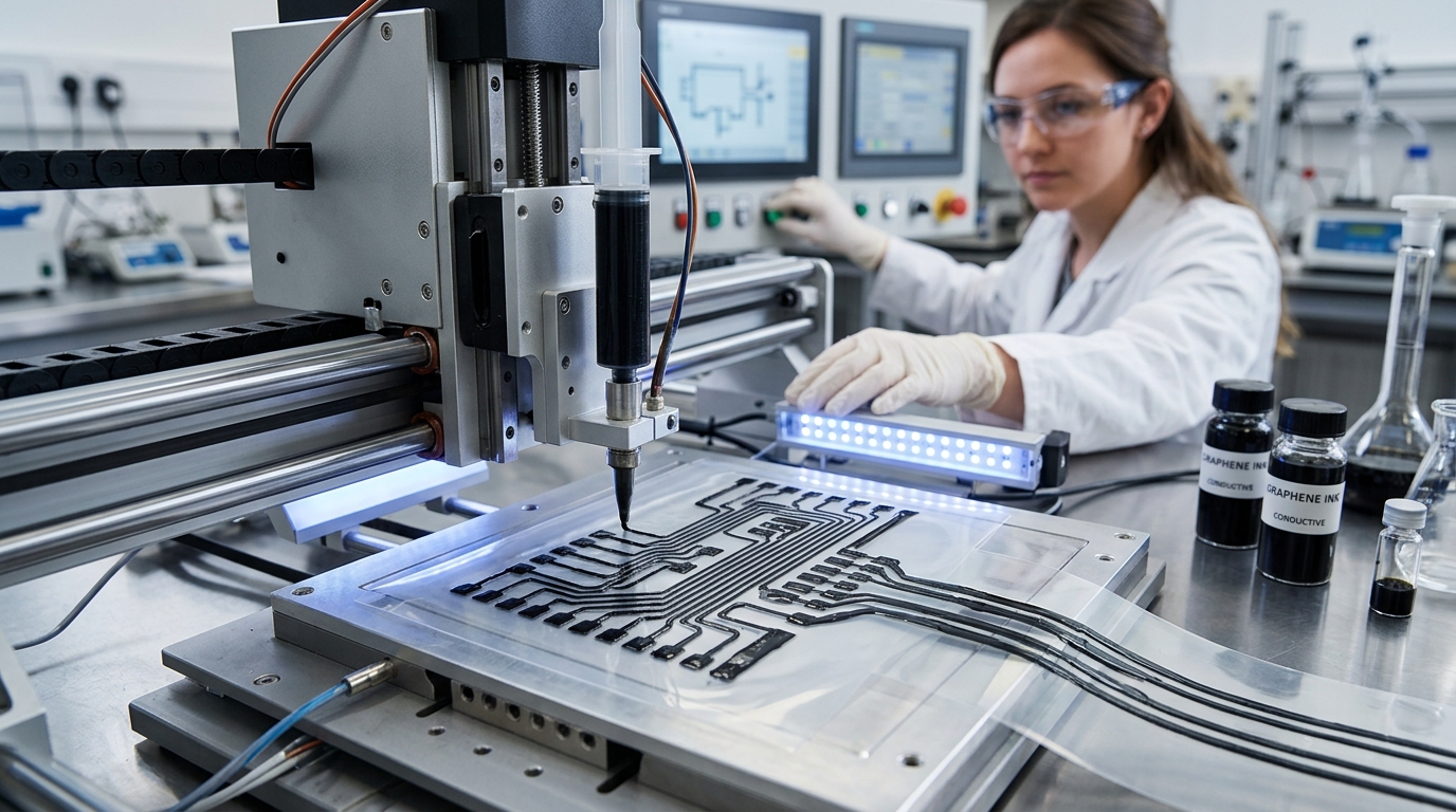
Coatings formulated with graphene provide barrier protection against corrosive ions such as chlorides. In marine and industrial infrastructure, zinc-rich primers enhanced with graphene decrease the overall zinc content needed while improving galvanic protection via improved electrical contact between zinc particles. In printed electronics, conductive graphene formulations are utilized for radio-frequency identification (RFID) antennas, flexible heaters, and biosensor test strips.
Technical Barriers to Commercial Scaling
Despite significant laboratory milestones since the mechanical isolation of graphene in 2004 and the subsequent Nobel Prize in 2010, wide-scale industrial deployment faces distinct engineering hurdles.
Dispersion and Re-agglomeration
Pristine graphene sheets experience strong van der Waals forces, causing individual flakes to spontaneously aggregate back into graphite-like bundles when mixed into solvents, resins, or molten polymers. Agglomeration eliminates the high surface area and aspect ratio that make nanomaterials desirable, creating localized defect points rather than reinforcement. Overcoming this requires optimized surface functionalization, masterbatch pre-dispersion, and specialized high-shear mixing equipment.
Standardization and Characterization
A persistent challenge in the market has been material inconsistency and ambiguous nomenclature. Materials marketed as graphene have often consisted of thick graphite flakes lacking nanoscale properties. The development of standardized frameworks by organizations such as the International Organization for Standardization (ISO) provides formal definitions based on layer count:
- Monolayer graphene: A single layer of sp2-hybridized carbon atoms.
- Bilayer and few-layer graphene: 2 to 10 distinct carbon layers.
- Graphite nanoplatelet / microplatelet: Carbon stacks exceeding 10 layers, up to 100 nm in thickness.
Without rigorous batch-to-batch characterization using Raman spectroscopy, atomic force microscopy (AFM), and transmission electron microscopy (TEM), industrial consumers face quality verification risks that complicate supply contracts.
Evaluation Criteria for Industrial Sourcing
Engineering and procurement teams evaluate graphene materials through a rigorous set of structural and chemical metrics rather than simple purity percentages.
- Lateral Flake Size: Dictates the aspect ratio; larger lateral dimensions generally lower the electrical percolation threshold but increase viscosity during melt processing.
- Layer Count and Thickness: Directly controls bending flexibility, optical absorption, and specific surface area.
- Defect Density (I_D/I_G Ratio): Measured via Raman spectroscopy, this ratio quantifies the disorder in the crystalline lattice. Low defect density indicates higher electrical and thermal performance, whereas higher defect density offers chemical attachment sites for polymer crosslinking.
- Oxygen Content and Heteroatom Doping: High residual oxygen indicates incomplete reduction or intentional functionalization, which influences dispersibility in polar versus non-polar matrix systems.
- Apparent Density and Surface Area: Brunauer-Emmett-Teller (BET) surface area measurements indicate the effective accessible area for electrochemical reactions or matrix bonding.
The Industrial Transition
The graphene sector is transitioning from an exploratory research phase into a specialized chemical additives and advanced materials industry. Commercial growth is driven not by replacing standard industrial materials outright, but by serving as an enabling additive that unlocks higher performance thresholds in existing systems. As international standards establish clearer quality baselines and automated continuous production methods mature, the focus of the market remains centered on precise material qualification, scalable dispersion engineering, and repeatable manufacturing economics.