Graphene Pencil
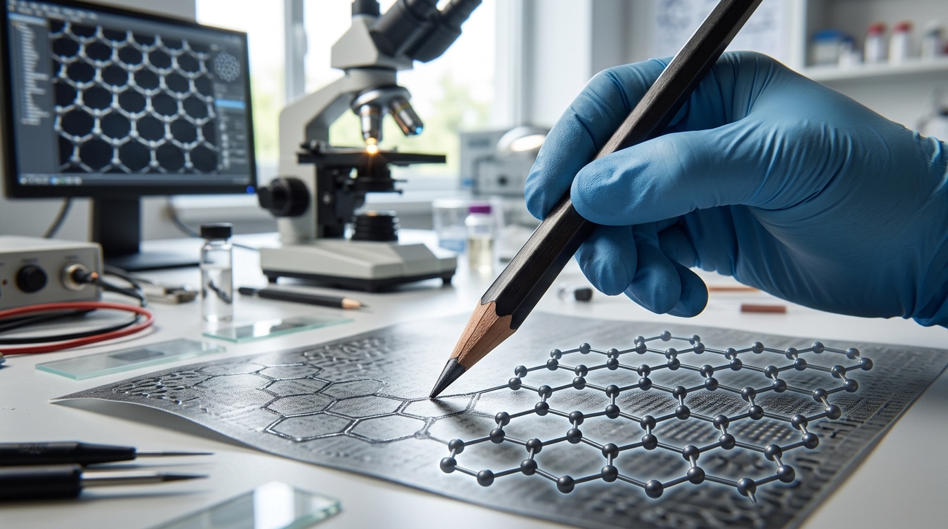
Every time a standard graphite pencil glides across a sheet of paper, it leaves behind microscopic fragments of carbon, including multilayer stacks and isolated flakes of graphene. The phrase graphene pencil refers to two closely linked concepts: the fundamental process of creating graphene-like carbon layers through mechanical friction with common pencils, and specialized drawing instruments engineered to deposit highly conductive, carbon-rich films for prototyping flexible electronics and chemical sensors.
While marketing claims sometimes blur the line between everyday art tools and advanced nanomaterials, the underlying physics is genuine. Drawing with a pencil is an act of mechanical exfoliation, shearing weakly bound layers of crystalline carbon across rough cellulose fibers to produce functional, conductive pathways without cleanrooms or toxic chemicals.
The Mechanics: How a Pencil Produces Graphene
To understand how a pencil generates graphene, one must look at the crystal lattice of graphite. Graphite consists of millions of stacked sheets of carbon atoms arranged in a flat, hexagonal honeycomb lattice. Within each sheet, carbon atoms share strong covalent bonds ($sp^2$ hybridization). However, the vertical layers are held together only by weak van der Waals forces.
When you press a pencil lead against paper and move it, two primary forces interact:
- Shear force: The lateral drag overcomes the weak interlayer van der Waals bonding, peeling microscopic platelets off the bulk crystal.
- Interfacial friction: The microscopic roughness of paper acts as a mechanical grater, trapping peeled carbon flakes within the porous network of cellulose fibers.
In 2004, physicists Andre Geim and Kostya Novoselov isolated single-layer graphene using adhesive tape to pull flakes from bulk graphite—a technique conceptually identical to the friction of a pencil mark. While a standard pencil stroke mostly leaves thick graphite chunks (tens to hundreds of layers thick), microscopic examination reveals numerous few-layer and multilayer graphene sheets distributed throughout the deposit.
The Pencil Grading Scale and Electrical Conductivity
Not all pencils deposit carbon equally. Standard pencil cores are not pure carbon; they are composite materials made from fine natural graphite powder, clay (primarily kaolin), and binding waxes or polymers. The ratio of graphite to clay defines the pencil’s hardness and darkness, universally classified on the European hardness scale (H to B).
| Pencil Grade | Graphite vs. Clay Ratio | Sheet Resistance Range | Typical Application in Electronics |
|---|---|---|---|
| 9H to 2H (Hard) | High clay, low graphite | Very High (> 10 MΩ/sq or insulating) | Dielectric spacers, high-value resistors |
| HB to F (Medium) | Balanced clay and graphite | Moderate (~100 kΩ/sq to 1 MΩ/sq) | General writing, basic pull-up resistors |
| 2B to 6B (Soft) | High graphite, low clay | Low (~5 kΩ/sq to 50 kΩ/sq) | Conductive traces, low-voltage circuits |
| 8B to 9B / Pure Graphite | Maximum graphite, minimal binder | Lowest (< 1 kΩ/sq to 5 kΩ/sq) | Electrodes, sensors, capacitive touch pads |
The transition from an insulating trace to an electrically conductive path follows the percolation threshold. In harder pencils, insulating clay particles physically separate the conductive graphite platelets, preventing electrons from flowing freely. In softer pencils (such as 6B through 9B), graphite flakes overlap continuously, establishing an uninterrupted conductive network across the paper surface.
Pencil-on-Paper Electronics (PPoE)
The ability to draw functional conductors directly onto paper has created a specialized research subfield known as pencil-on-paper electronics. By treating the graphite trace as an active material and ordinary paper as a flexible, biodegradable substrate, researchers and engineers build rapid prototypes of low-cost electrical devices.
1. Mechanical Strain and Flex Sensors
When a pencil trace on paper is bent outward (convex bending), tensile strain pulls the overlapping carbon flakes slightly apart. This increases the contact resistance between neighboring platelets, causing the overall resistance of the line to spike. When bent inward (concave bending), compression forces the flakes tighter together, reducing resistance.
Because paper is flexible and lightweight, a simple drawn line serves as an effective piezoresistive strain gauge for monitoring structural deflection, human joint movement, or subtle vibrations.
2. Chemical and Gas Sensors
The edges of sheared graphene and graphite flakes feature unsaturated carbon bonds, functional oxygen groups, and defect sites. These active sites readily adsorb gaseous molecules such as nitrogen dioxide ($NO_2$), ammonia ($NH_3$), and volatile organic compounds (VOCs). Adsorption alters the local carrier density of the carbon lattice, triggering a measurable shift in electrical resistance that correlates with gas concentration.
3. Chemiresistive and Electrochemical Electrodes
By drawing dense carbon pads onto paper, users can fabricate three-electrode electrochemical cells (working, counter, and reference electrodes) at negligible cost. These pencil electrodes have demonstrated reliable performance in detecting heavy metals, glucose, and hydrogen peroxide in aqueous solutions, offering a disposable platform for point-of-care diagnostics in resource-limited environments.
4. Passive RFID and Capacitive Interfaces
Because pencil traces exhibit stable capacitive responses when approached by human skin, drawn patterns can act as capacitive touch switches, volume sliders, or keypads on cardboard packaging. When patterned into resonant spiral geometries, highly conductive carbon tracks can function as passive high-frequency antennas and filters.
Commercial Graphene Pencils vs. Standard Art Supplies
The growing interest in nanomaterials has led manufacturers to market specialized products under the label of graphene pencils or conductive carbon pens. Understanding the material composition prevents common misconceptions.
Standard Artist Pencils
Traditional wood-cased graphite pencils use naturally mined or synthetic graphite mixed with clay binders and fired in kilns. While they do deposit few-layer graphene flakes during writing, the deposit is a heterogeneous mixture dominated by bulk graphite micro-particles and clay matrix residues. They are inexpensive and widely available, but offer moderate conductivity and lower trace uniformity.
Engineered Conductive & Graphene-Enriched Pencils
Modern conductive drawing instruments replace traditional clay with conductive polymeric binders or combine high-purity, pre-exfoliated graphene nanoplatelets with finely ground graphite. These formulations exhibit critical advantages:
- Lower sheet resistance: Traces achieve higher conductivity with fewer passes because the binder does not act as an electrical insulator.
- Superior adhesion: Advanced binders prevent the flaking and smudging typical of soft 9B artist pencils.
- Trace uniformity: Formulations are optimized to deposit a continuous carbon film with minimal micro-voids, ensuring consistent electrical properties across the entire length of the trace.
Material Tradeoffs and Practical Limitations
While the concept of drawing circuits with a pencil is compelling, severe physical and material constraints prevent pencil traces from replacing copper wires, etched printed circuit boards (PCBs), or vacuum-deposited thin films in high-performance electronics.
High Sheet Resistance
Even the most concentrated, heavily burnished graphite-pencil trace has a sheet resistance orders of magnitude higher than bulk metals. A copper trace on a PCB exhibits a sheet resistance measured in milliohms per square, whereas a dense 9B pencil line typically yields hundreds to thousands of ohms per square. Consequently, pencil circuits cannot carry substantial electrical current without experiencing severe voltage drops and resistive heating.
Substrate Roughness and Porosity
The physical structure of paper dictates trace quality. Highly porous, textured watercolor paper yields fragmented, discontinuous deposits. Smooth, calendered papers or coated parchment provide higher continuity and conductivity, but smooth surfaces offer fewer mechanical anchor points, making the trace susceptible to abrasion and detachment.
Environmental Degradation
Pencil traces lack a protective passivation layer. Direct exposure to ambient humidity, atmospheric oxygen, and skin oils alters the trace’s baseline resistance over time. For sensor applications, this causes signal baseline drift that requires baseline calibration before every measurement.
Best Practices for Creating Conductive Pencil Traces
For educational demonstrations, rapid sensor prototyping, or hobby electronics, following specific preparation methods dramatically improves electrical performance:
- Select the correct grade: Use pencil grades between 6B and 9B, or woodless pure-graphite sticks, to maximize the carbon-to-binder ratio.
- Choose dense, smooth paper: Calendered cardstock, glossy photo paper, or weighing paper offers the best balance of smoothness and mechanical grip.
- Burnish with multiple passes: Draw the line repeatedly over the same path. Overlapping strokes fill micro-cavities, increase flake packing density, and reduce sheet resistance by up to 80%.
- Secure electrical interfaces: Standard alligator clips can tear paper and crack the carbon film. Secure interface leads using conductive copper tape, silver epoxy, or spring-loaded flat contacts.
- Encapsulate against wear: Spraying or laminating the trace with a clear acrylic or polyurethane sealant protects the carbon layer from abrasion and moisture without altering its static resistive properties.
The Role of Pencil-Derived Carbon in Materials Science
The graphene pencil illustrates an essential truth of materials science: sophisticated nanoscale phenomena do not always require multi-million-dollar synthesis reactors. The mechanical friction of graphite against paper provides a reliable, accessible bridge between macroscopic mechanics and two-dimensional nanomaterials.
While pencil traces cannot replace metallic interconnects in modern computing hardware, they remain a premier tool for educational exploration, rapid green prototyping, disposable diagnostics, and low-power sensory devices. By leveraging the natural shear properties of stacked carbon sheets, the humble pencil continues to serve as both an artistic instrument and a functional gateway to 2D materials.