Graphene Films
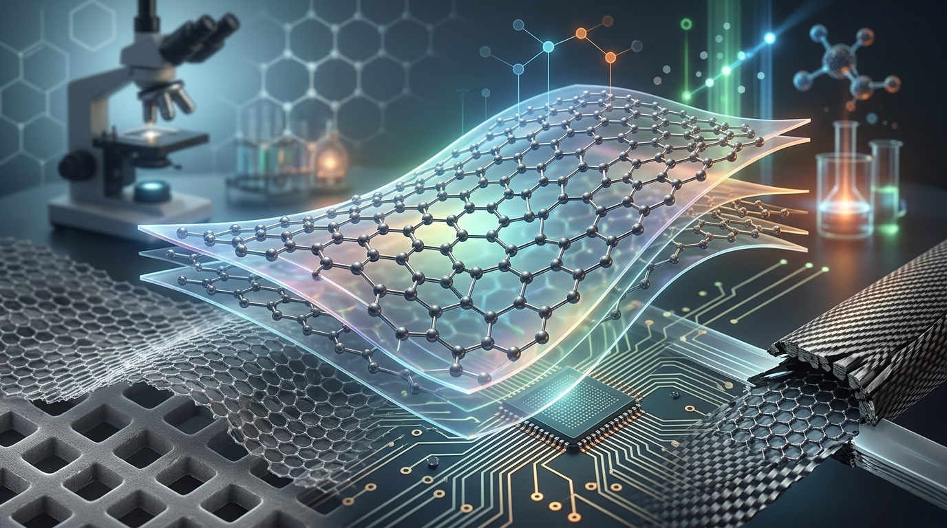
Graphene films are macroscopic, two-dimensional carbon layers engineered for integration onto functional substrates. Unlike discontinuous graphene nanoplatelets, powders, or bulk additives blended into polymer masterbatches, graphene films are continuous or semi-continuous planar architectures whose value derives from uninterrupted in-plane sp2-hybridized carbon networks. These films enable applications requiring high optical transparency, electrical conductivity, barrier impermeability, and thermal dissipation across macroscopic surface areas.
Understanding the engineering landscape of graphene films requires distinguishing between synthesis routes, transfer methodologies, structural layer counts, and practical manufacturing challenges. While pristine monolayer sheets offer exceptional physical limits, practical implementation depends on balancing performance characteristics with scalable production economics.
Classification of Graphene Films
Graphene films are classified by their atomic thickness, crystalline continuity, and manufacturing morphology. These architectural factors determine whether a film behaves as a ballistic electronic conductor, an impermeable atomic barrier, or an interconnected percolation network.
Continuous Planar Films
Continuous planar films are synthesized directly via vapor-phase reactions or epitaxial crystallization to produce uninterrupted, sheet-like morphologies across macroscopic dimensions:
- Monolayer Graphene Films: A single atom-thick carbon layer exhibiting theoretical optical transmittance of approximately 97.7% (absorbing roughly 2.3% of incident white light) and high intrinsic charge carrier mobility. Monolayers are primarily utilized in high-frequency field-effect transistors, optoelectronics, and precision sensor interfaces.
- Few-Layer Graphene (FLG) Films: Consisting of 2 to 5 stacked graphene sheets. FLG films balance optical transparency (attenuating an additional ~2.3% per layer) with lower sheet resistance compared to monolayers, reducing the impact of substrate-induced scattering and local pinhole defects.
- Multilayer Graphene Films: Composed of 6 to 10 layers. Beyond roughly 10 layers, the electronic band structure closely resembles bulk graphite. These thicker films are deployed predominantly in thermal spreading, electromagnetic interference (EMI) shielding, and robust barrier coatings where optical transparency is secondary to electrical or thermal conductance.
Solution-Processed and Flake Thin Films
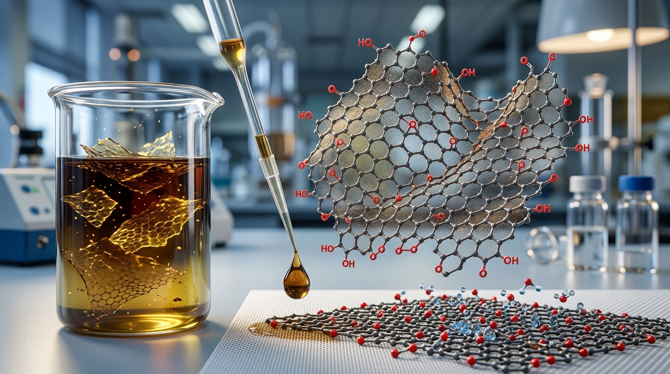
Distinct from continuous crystalline sheets, solution-processed graphene thin films are assembled from colloidal suspensions of graphene oxide (GO), reduced graphene oxide (rGO), or liquid-phase exfoliated (LPE) nanosheets. These films are deposited onto substrates via spray coating, spin coating, dip coating, or slot-die coating.
Because they consist of overlapping, randomly oriented flakes, their charge transport is governed by inter-flake contact resistance and variable-range hopping across defect sites. While mechanically flexible and significantly cheaper to produce over large areas, their electrical and thermal conductivities are orders of magnitude lower than continuous chemical vapor deposition (CVD) films.
| Metric / Feature | CVD Continuous Films | Solution-Processed Flake Films |
|---|---|---|
| Morphology | Continuous, polycrystalline atomic sheet | Overlapping network of individual flakes |
| Typical Thickness | 1 to 3 layers (sub-nanometer to ~1 nm) | 10 nm to several micrometers |
| Sheet Resistance (Rs) | 100 – 1,000 Ω/sq (doped: <50 Ω/sq) | 103 – 106 Ω/sq (post-reduction) |
| Optical Transmittance | >90% to 97.7% | 60% – 85% (at comparable conductivity) |
| Carrier Mobility | 1,000 – 10,000+ cm2/(V·s) on target substrates | 0.1 – 50 cm2/(V·s) |
| Primary Use Cases | Semiconductors, high-end displays, photonic devices | Antistatic coatings, basic heating elements, EMI shielding |
Primary Synthesis and Fabrication Techniques
Industrial deployment of continuous graphene films depends on scalable synthesis methods capable of controlling defect density, domain size, and layer uniformity across vast surface areas.
Chemical Vapor Deposition (CVD) on Metal Foils
Thermal CVD is the predominant method for synthesizing large-area, continuous graphene films. In this process, a carbon-bearing gaseous precursor (typically methane, CH4) is introduced into a high-temperature reactor (900°C to 1050°C) alongside hydrogen and an inert carrier gas over a catalytic transition metal foil.
- Copper (Cu) Foils: Copper exhibits low carbon solubility. The growth mechanism is self-limiting and surface-mediated: once the copper surface is fully nucleated and covered by a monolayer of carbon atoms, catalytic decomposition of methane halts. This produces predominantly uniform monolayer films with controlled grain sizes.
- Nickel (Ni) Foils: Nickel exhibits high carbon solubility at elevated temperatures. Carbon dissolves into the nickel bulk during exposure and subsequently segregates/precipitates out to the surface during cooling. Controlling layer uniformity on nickel is challenging, often yielding inhomogeneous mixtures of few-layer and multilayer domains, though it is advantageous for intentional multilayer growth.
Roll-to-Roll (R2R) Continuous Growth
To reduce manufacturing costs, industrial facilities employ continuous roll-to-roll (R2R) CVD reactors. Flexible copper foil is unspooled, passed through heating zones where graphene nucleates continuously, and rewound onto collection spools. Managing thermal gradients, foil tension, and dynamic gas flow dynamics within R2R reactors is critical to avoid micro-tearing and preserve film uniformity across meter-wide webs.
Epitaxial Growth on Silicon Carbide (SiC)
Epitaxial growth bypasses metal catalysts by thermally decomposing single-crystal silicon carbide (SiC) wafers at high temperatures (typically 1200°C to 1600°C) under vacuum or an argon atmosphere. Silicon atoms sublime from the surface, leaving behind residual carbon atoms that self-assemble into graphene layers.
Growth on the silicon-terminated face (0001) produces uniform, wafer-scale monolayers over a buffer layer, whereas growth on the carbon-terminated face (000-1) yields thicker, rotationally faulted multilayer stacks. Although this technique produces high electronic quality without post-growth transfer steps, the high cost of SiC substrates confines it primarily to specialized radio-frequency (RF) and quantum metrology devices.
Substrate Transfer and Handling Protocols
Because CVD graphene is synthesized on metallic foils, it must usually be transferred onto target dielectric substrates—such as silicon dioxide, quartz, polyethylene terephthalate (PET), or glass—to serve in electronic or optical components. The transfer process represents the primary source of structural damage and contamination in film manufacturing.
Polymer-Assisted Wet Chemical Etching
The standard laboratory and pilot-scale transfer method relies on a supportive sacrificial polymer:
- A thin film of poly(methyl methacrylate) (PMMA) or thermal release tape is spin-coated or laminated onto the graphene/copper stack.
- The underlying copper substrate is chemically dissolved in an etchant bath (such as ammonium persulfate, iron(III) chloride, or copper chloride).
- The remaining PMMA/graphene membrane is rinsed in deionized water to remove residual metallic salts.
- The floating membrane is mechanically scooped onto the target substrate and dried.
- The polymer support is dissolved using organic solvents (such as acetone).
While straightforward, wet etching destroys the expensive metal growth foil and leaves residual polymer contamination on the graphene surface that degrades carrier mobility and increases contact resistance.
Electrochemical Delamination (Bubbling Transfer)
To preserve and reuse the metallic growth substrate, electrochemical delamination utilizes the graphene/metal stack as a cathode in an aqueous electrolyte cell. Applying a small voltage drives the electrolysis of water, generating hydrogen gas bubbles at the interface between the metal foil and the graphene sheet.
The mechanical pressure exerted by the nucleating bubbles gently detaches the graphene film (supported by a carrier layer) from the metal substrate. This method leaves the metal foil intact for subsequent growth cycles and significantly shortens processing time, although localized bubble expansion can induce micro-cracks if voltage and withdrawal rates are not precisely controlled.
Dry Roll-to-Roll Lamination and Delamination
For high-throughput flexible electronics, continuous dry transfer avoids liquid chemical baths. The CVD graphene-on-copper foil is laminated directly against a flexible target substrate coated with a thermal or ultraviolet-curable adhesive. As the layered structure passes through controlled pressure rollers, differential surface energy or mechanical peeling separates the graphene from the copper foil, transferring it directly onto the polymer film in a continuous web.
Key Performance Properties and Engineering Metrics
The operational suitability of graphene films depends on several interlinked physical and electrical properties that must be balanced for specific applications.
Optical Transmittance and Sheet Resistance
For optoelectronic electrodes, continuous graphene films are judged by the trade-off between transparency and electrical conductance. While an intrinsic monolayer possesses a sheet resistance ranging from 500 to several thousand ohms per square (Ω/sq) alongside 97.7% optical transmittance, commercial transparent conductive electrodes (TCEs) generally require sheet resistance values below 50–100 Ω/sq with total transmittance exceeding 85–90%.
To reach these electrical thresholds, manufacturers employ chemical doping (using nitric acid, gold(III) chloride, or bis(trifluoromethanesulfonyl)imide) or stack 2 to 4 layers together. Doping shifts the Fermi level, dramatically increasing charge carrier concentration and reducing sheet resistance without substantially degrading optical clarity.
Carrier Mobility
In clean, suspended monolayer graphene, carrier mobility can exceed 200,000 cm2/(V·s) at low temperatures. However, when integrated into commercial film formats on practical substrates like SiO2 or flexible polymers, room-temperature mobility typically ranges between 1,000 and 10,000 cm2/(V·s). Scattering from charged surface impurities, substrate optical phonons, and film domain boundaries limits the mobility, though it remains significantly higher than that of amorphous silicon or standard conductive oxides.
Mechanical Flexibility and Fatigue Resistance
Continuous graphene films possess an intrinsic breaking strength of 42 N/m and a Young’s modulus near 1.0 TPa. In thin-film form, they withstand extensive mechanical strain (typically up to 6–10% elastic strain before structural failure) and hundreds of thousands of bending cycles around millimeter radii without critical loss of electrical continuity. This resilience sharply contrasts with brittle metal oxides like indium tin oxide (ITO), which develop micro-fractures under minimal strain.
Barrier Impermeability
Pristine, defect-free graphene lattices are completely impermeable to all standard gas molecules, including helium. In multi-layer film form, this barrier functionality inhibits the permeation of moisture, oxygen, and corrosive volatile compounds, making high-quality graphene films prime candidates for ultra-thin environmental passivation layers.
Inspection and Metrology Techniques
Accurate process control in film fabrication requires rapid, non-destructive characterization across large areas to verify continuity, layer count, and crystalline quality.
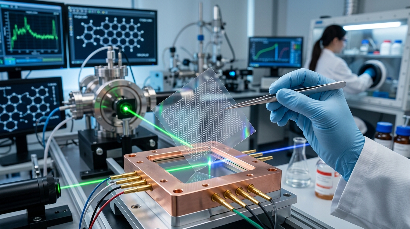
- Raman Spectroscopy: The standard analytical benchmark for graphene films. The intensity ratio of the 2D peak (~2680 cm-1) to the G peak (~1580 cm-1), alongside the 2D peak’s full width at half maximum (FWHM), identifies monolayer versus few-layer structures. The presence and magnitude of the D peak (~1350 cm-1) quantitatively reveals the density of point defects, grain boundaries, and functionalization sites.
- Atomic Force Microscopy (AFM): Provides nanometer-scale topographic mapping to confirm film thickness, identify polymer transfer residues, inspect surface roughness, and locate mechanical tears or folds.
- Four-Point Probe and Terahertz Time-Domain Spectroscopy (THz-TDS): Contact-based four-point probes measure sheet resistance directly across the surface. Non-contact THz-TDS maps sheet conductance and carrier mobility non-destructively across full wafers or roll-to-roll webs at industrial line speeds.
Major Industrial and Commercial Applications
Graphene films have transitioned from basic laboratory phenomena to qualified commercial and pre-commercial components across multiple engineering domains.
Transparent Conductive Electrodes (TCEs)
Graphene films serve as non-brittle, non-reflective alternative electrodes for resistive and capacitive touchscreens, organic photovoltaics (OPVs), and organic light-emitting diode (OLED) displays. While traditional indium tin oxide (ITO) suffers from market-driven material supply volatility and brittle failure under flexure, doped CVD graphene films provide structural compliance and neutral optical absorption profiles across both visible and infrared spectrums.
Flexible High-Frequency Electronics
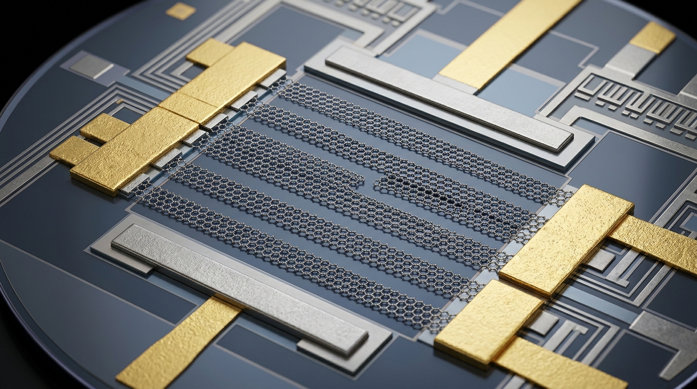
Due to high field-effect mobility and thin profiles, continuous graphene films are utilized in flexible radio-frequency (RF) transistors, wearable antennas, and electromagnetic interference (EMI) attenuation layers. Graphene field-effect transistors (GFETs) operate at gigahertz switching frequencies on flexible plastic substrates, enabling lightweight communication interfaces and ultra-sensitive biosensing channels.
Thermal Spreading Films
As microprocessors, power modules, and compact electronics increase in heat flux density, thermal dissipation becomes a central bottleneck. Thick, highly oriented multilayer graphene films exhibit in-plane thermal conductivities exceeding 1,000 W/(m·K)—outperforming conventional copper foils (roughly 400 W/(m·K)) and aluminum alloys. When placed adjacent to heat sources, these films spread concentrated heat laterally, eliminating hot spots and preventing localized thermal throttling.
Protective Barriers and Anti-Corrosion Coatings
Continuous few-layer graphene films applied to metal interconnects or sensitive optoelectronic materials serve as passivation barriers. Because they resist atomic diffusion and withstand high environmental temperatures, these coatings mitigate galvanic corrosion, prevent metal oxidation, and extend the operating lifetimes of underlying circuits without changing physical component dimensions.
Separation and Desalination Membranes
Engineered graphene films containing deliberately created sub-nanometer nanopores act as atomic-scale sieves. Because the film is only one or few atoms thick, hydraulic resistance is minimized compared to thick polymer membranes, driving high liquid and gas permeation rates while selectively blocking salt ions, biological pathogens, or heavy metals.
Commercial Readiness Overview Across Sectors
The industrial adoption of graphene films varies across sectors, determined by the acceptable cost per square meter and required crystalline perfection:
- Thermal Management Films: High Commercial Adoption. Thicker, multi-layer films or compacted graphite-graphene hybrid sheets are widely deployed inside consumer smartphones and small electronics where cost models support them and defect tolerance is relatively broad.
- Touchscreens and Capacitive Sensors: Moderate Commercial Adoption. Flexible touch panels using multi-layer or hybrid metal grid/graphene films have reached commercial production, primarily serving niche flexible or ruggedized display units.
- Corrosion and Environmental Barriers: Pilot to Early Commercialization. Barrier coatings are qualified for specialized electronics packaging, though long-term integrity depends on completely eliminating pinhole defects.
- High-End Logic and RF Semiconductors: Research and Development / Pilot Demonstration. The absence of an intrinsic electronic bandgap in pristine graphene limits its use in classical digital logic circuits (where high on/off current ratios are mandatory), confining advanced electronic deployment primarily to analog RF devices, mixers, photodetectors, and biosensors.
Technical and Manufacturing Bottlenecks
Despite substantial progress in synthesis capacity, widespread industrial use of continuous graphene films faces distinct manufacturing hurdles.
Grain Boundaries and Polycrystallinity
Standard CVD growth on metal foils yields polycrystalline films composed of stitching individual grains. The boundaries between these crystalline domains contain pentagon-heptagon dislocation loops, disordered carbon arrangements, and dangling bonds. These grain boundaries scatter charge carriers, act as initial points of mechanical failure under tension, and provide diffusion pathways for corrosive gases, degrading electrical, mechanical, and barrier performance relative to single-crystal benchmarks.
Wrinkles, Folds, and Pinholes
During the cooling phase of high-temperature CVD growth, differences in thermal expansion coefficients between the metal foil (which contracts significantly) and the graphene film (which displays a negative thermal expansion coefficient over parts of the range) generate compressive stress. This stress relaxes through the formation of surface ripples, wrinkles, and folds. Subsequent mechanical handling or transfer introduces pinholes and micro-cracks that compromise the film’s atomic barrier properties.
Transfer-Induced Chemical Contamination
Removing sacrificial polymer supports leaves thin, nanometer-scale residues across the graphene film. These residues induce p-type doping, cause unintentional charge carrier scattering, increase interfacial contact resistance, and hinder clean contact with subsequently deposited dielectric layers. Wet-chemical cleanings and thermal annealing mitigate this contamination but can introduce defect sites and increase overall manufacturing cycle times.
Yield Economics and Production Costs
While raw chemical precursors (methane, hydrogen) are inexpensive, the cumulative operational expenditures of graphene film manufacturing—including high-vacuum furnace operation, thermal energy consumption, sacrificial metal foil etching, continuous substrate cleanups, and cleanroom handling—keep production costs significantly higher than traditional solution-cast polymers or sputtered thin films. Industrial success hinges on closed-loop, non-destructive foil reuse systems and dry, roll-to-roll transfer operations that maximize throughput while maintaining defect densities within acceptable tolerances.