Graphene Properties
Graphene properties derive directly from its nature as an isolated, single-atom-thick layer of carbon atoms arranged in a two-dimensional honeycomb crystal lattice. First experimentally isolated in 2004 via mechanical exfoliation, this two-dimensional allotrope of carbon exhibits an unprecedented combination of mechanical stiffness, electrical mobility, thermal conductance, optical transmittance, and molecular impermeability. Because every atom in monolayer graphene is a surface atom, its bulk behavior is dictated entirely by quantum mechanical confinement and interfacial chemistry, establishing physical benchmarks across materials science.
Crystal Lattice and Electronic Band Structure
Graphene is constructed from carbon atoms covalently bonded via planar sp2 hybridization. Each carbon atom forms three robust in-plane sigma (σ) bonds with neighboring atoms at a bond length of approximately 0.142 nanometers (nm), separated by 120-degree angles. The underlying unit cell is non-Bravais, comprising a two-atom basis designated as sublattices A and B. The lattice vectors define a hexagonal unit cell with a lattice constant of a = 0.246 nm.
Perpendicular to the basal plane, the remaining half-filled 2pz orbitals overlap across adjacent atomic sites to establish a delocalized network of pi (π) and pi-star (π*) bands. This conjugated π-electron system governs the material’s low-energy electronic behavior. The conduction band (π*) and valence band (π) meet symmetrically at six points located at the corners of the hexagonal Brillouin zone, known as the Dirac points (K and K’ valleys).
Near these intersection points, the energy-momentum dispersion relation is linear rather than parabolic: E(κ) = ±ℏvF|κ|, where ℏ is the reduced Planck constant, κ is the wavevector measured relative to the Dirac point, and vF represents the Fermi velocity (approximately 1 × 10⁶ m/s). Because of this linear dispersion, charge carriers in pristine monolayer graphene behave mathematically as massless relativistic Dirac fermions, leading to novel quantum phenomena including an anomalous room-temperature quantum Hall effect and the absence of backscattering (Klein tunneling).
Mechanical Properties and Elastic Limits
The planar σ-bonds established by carbon sp2 orbitals are among the strongest known covalent bonds in chemistry, providing pristine monolayer graphene with unmatched mechanical parameters.
- Intrinsic Tensile Strength: Monolayer graphene has a theoretical and experimentally verified intrinsic breaking strength of approximately 130 GPa (equivalent to ~42 N/m for a 2D sheet). This figure makes defect-free graphene approximately 100 to 200 times stronger than structural steel of equivalent thickness.
- Young’s Modulus: Graphene exhibits an in-plane Young’s modulus (elastic modulus) of ~1.0 TPa (equivalent to a 2D stiffness of ~340 N/m), demonstrating extreme resistance to elastic deformation.
- Breaking Strain: Pristine graphene can sustain elastic strains exceeding 15% to 25% before undergoing irreversible brittle fracture, far exceeding conventional crystalline metals and ceramics, which typically yield at strains under 1% to 2%.
These mechanical metrics are typically quantified experimentally through atomic force microscopy (AFM) nanoindentation over suspended circular micro-cavities. When free of atomic vacancies and grain boundaries, graphene deforms non-linearly under high loads according to high-order elastic constants before catastrophic failure.
In macroscale sheets produced by chemical vapor deposition (CVD), mechanical performance is governed by Griffith’s fracture mechanics. Grain boundaries, topological Stone-Wales defects, and point vacancies concentrate local stresses, lowering the practical tensile strength of polycrystalline graphene to between 30 and 70 GPa depending on average grain size.
Electrical Transport and Carrier Dynamics
Graphene is classified as a zero-bandgap semimetal (or zero-overlap semimetal). At thermodynamic equilibrium and neutral gate voltage (the Dirac point), the density of electronic states vanishes, yet carrier concentration does not fall to zero due to thermally excited carriers and localized charge puddles induced by substrate impurities.
Carrier Mobility
Because low-energy carriers lack effective mass, graphene facilitates rapid electronic transport:
- Suspended Monolayers: When suspended in vacuum or cryogenic conditions to minimize substrate phonon interaction, intrinsic carrier mobility can exceed 200,000 cm2/(V·s) at carrier densities around 1011 cm-2. Theoretical ballistic limits governed purely by acoustic phonon scattering predict room-temperature upper limits near 250,000 cm2/(V·s).
- Substrate-Supported Monolayers: Deposition onto typical substrates introduces scattering mechanisms. On conventional silicon dioxide (SiO2), charged surface state impurities, surface roughness, and remote optical phonon scattering depress mobility to roughly 10,000–20,000 cm2/(V·s). Hexagonal boron nitride (h-BN) encapsulation largely preserves intrinsic properties, enabling room-temperature mobilities approaching 100,000 cm2/(V·s).
Ballistic Conduction and Ambipolar Field Effect
At sub-micron channel lengths, electron mean free paths in high-purity graphene can reach hundreds of nanometers to several micrometers at room temperature. This enables ballistic conduction, where electrons traverse the conducting channel without scattering from crystal defects or impurities.
Applying an electrostatic gate allows continuous tuning of the carrier type and concentration from electrons to holes across the Dirac neutrality point, producing an ambipolar field effect. However, the absence of an intrinsic electronic bandgap results in poor current on/off ratios (typically < 10 at room temperature) in field-effect configurations, presenting a barrier to classical digital logic circuits without further structural modification.
Bandgap Engineering and Modulation
To overcome the zero-bandgap limitation, several strategies are employed:
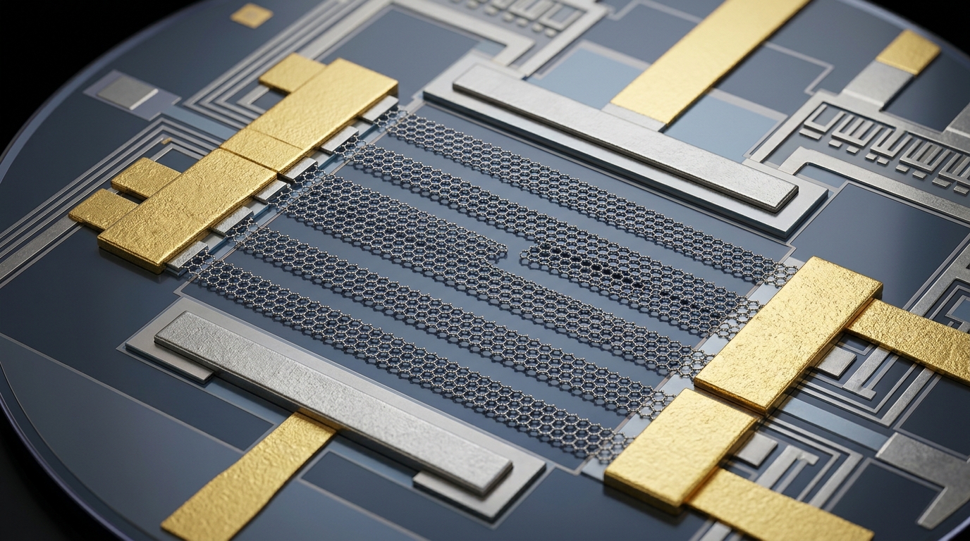
- Quantum Confinement: Patterning graphene into narrow ribbons (graphene nanoribbons, or GNRs) with widths below 10 nm opens a bandgap inversely proportional to width, though edge roughness frequently suppresses carrier mobility.
- Bilayer Displacement Fields: Applying an out-of-plane electric field across an AB-stacked (Bernal) bilayer breaks inversion symmetry, opening a gate-tunable bandgap of up to 250 meV.
- Twistronics: Twisting stacked graphene sheets relative to each other at specific rotation angles (such as the “magic angle” of ~1.1 degrees for bilayers) alters the Dirac dispersion, yielding flat bands that induce strongly correlated electron behaviors and unconventional superconductivity.
- Chemical Doping: Covalent functionalization (e.g., fluorination, hydrogenation to form graphane) or non-covalent molecular adsorption shifts the Fermi level and alters hybridization, though often at the expense of electron mobility.
Thermal Transport Properties
Thermal dissipation in carbon nanomaterials is dominated by lattice vibrations (phonons) rather than electronic conduction, with electrons contributing less than 1% to overall thermal transport under normal conditions.
Suspended monolayer graphene displays room-temperature in-plane thermal conductivity (κ) ranging from 3,000 to 5,000 W/(m·K), far exceeding diamond (~2,000 W/(m·K)) and bulk copper (~400 W/(m·K)). This high thermal conductance stems from the long mean free paths of acoustic phonons: longitudinal acoustic (LA), transverse acoustic (TA), and flexural out-of-plane acoustic (ZA) modes.
Because out-of-plane flexural modes are energetically accessible and weakly scattered in suspended configurations, they serve as substantial heat carriers. However, when graphene rests directly on a substrate (such as SiO2), clamping and interface bonding suppress the out-of-plane flexural modes and induce Umklapp scattering, reducing room-temperature thermal conductivity to approximately 600–1,000 W/(m·K). Despite this reduction, substrate-supported graphene remains among the most thermally conductive interface coatings known.
Optical Characteristics
Despite being only one atom thick (nominal thickness ~0.335 nm), monolayer graphene interacts strongly with incident photons across spectral ranges extending from the ultraviolet to the far-infrared.
For normal incident light in the visible spectrum, the optical absorption of monolayer graphene is defined primarily by the fine-structure constant (α = e2/(ℏc) ≈ 1/137). The sheet absorption is given by A = πα ≈ 2.293%, corresponding to an optical transparency of approximately 97.7%.
Because the low-energy electronic bands are linear and symmetric, interband absorption remains virtually constant across the visible spectrum, yielding a neutral gray, spectrally flat optical absorption profile. As additional layers are stacked, absorption increases linearly: each layer adds roughly 2.3% absorption up to few-layer thicknesses.
Under high optical excitation intensities, graphene exhibits saturable absorption due to Pauli blocking, wherein photo-excited electrons fill available states at the conduction band edge, preventing further absorption. This nonlinear property makes graphene useful for ultrafast passively mode-locked fiber lasers. Furthermore, graphene supports highly confined 2D surface plasmons in the terahertz and mid-infrared regimes, exhibiting significantly lower losses and greater electrostatic tunability than noble-metal plasmonic systems.
Chemical and Barrier Properties
Basal Plane Inertness vs. Edge Reactivity
The basal plane of pristine graphene is chemically inert. The localized σ-bonds satisfy carbon valence requirements, and the delocalized π-electron cloud forms a low-energy aromatic continuum that resists chemical attack by ambient oxygen, acids, and bases at moderate temperatures.
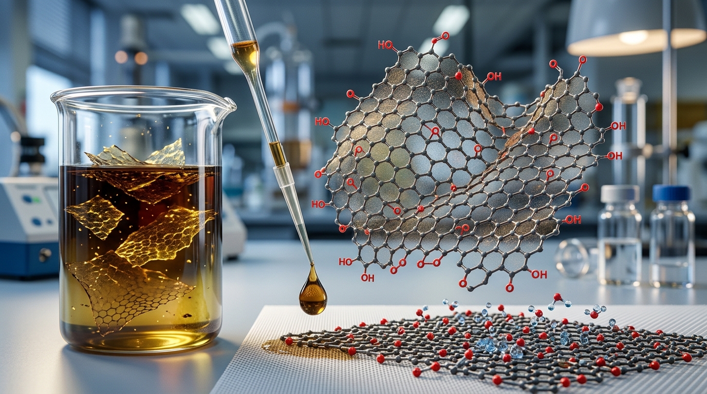
In contrast, regions of broken symmetry—such as crystal edges (zigzag and armchair configurations), grain boundaries, point vacancies, and atomic dislocations—feature dangling bonds and elevated local densities of states. Consequently, chemical functionalization (including oxidation, halogenation, and radical addition) initiates preferentially at edge sites and defective coordinates. Transforming carbon from sp2 to sp3 geometry puckers the planar lattice, locally distorting electrical and mechanical attributes.
Molecular and Gas Impermeability
The electron cloud formed by overlapping carbon π-orbitals creates an overlapping repulsive electrostatic potential across the six-membered aromatic carbon rings. The geometric pore aperture within the ring is under 0.1 nm, whereas the kinetic diameter of even the smallest noble gas atom (helium) is approximately 0.26 nm.
As a result, pristine, defect-free monolayer graphene is strictly impermeable to all standard gases and liquids at ambient pressure and temperature. Helium gas under pressure cannot diffuse across a defect-free basal plane. Sub-nanometer pores must be introduced lithographically or chemically (e.g., via ion bombardment or oxidative etching) to enable size-selective molecular sieving, gas separation, or water desalination.
Analytical Characterization Methods
Accurate verification of graphene properties relies on specialized characterization techniques:
- Raman Spectroscopy: The primary non-destructive tool for evaluating layer count, strain, and defect density. Pristine monolayer graphene features two prominent signatures: the G band (~1582 cm-1), representing the primary in-plane vibrational mode, and the 2D band (historically G’, ~2680 cm-1), an overtone of momentum-conserving phonon scattering. A sharp, symmetric 2D peak with an intensity ratio I2D/IG > 2 indicates high-quality monolayer graphene. The D band (~1350 cm-1) requires a structural defect for momentum conservation; the ratio ID/IG directly quantifies atomic defect density.
- Atomic Force Microscopy (AFM): Provides spatial height profiles. Due to surface adsorption and chemical contrast with underlying substrates, monolayer graphene typically yields an apparent AFM height of 0.5 to 1.0 nm on SiO2, despite its nominal crystallographic spacing of 0.335 nm. AFM nanoindentation over micro-etched cavities measures quantitative elastic moduli and rupture stress.
- Hall Bar Geometries and van der Pauw Measurements: Standard solid-state configurations used to extract sheet resistance (Rs), carrier density (n), and Hall mobility (μ) by applying perpendicular magnetic fields at variable temperatures.
Comparative Performance Metrics
The properties of graphene change markedly as additional atomic planes are stacked, transitioning from a strictly two-dimensional Dirac semimetal toward bulk highly oriented pyrolytic graphite (HOPG).
| Parameter | Monolayer (Theoretical) | Monolayer (Experimental CVD/Exfoliated) | Bilayer (Bernal AB-Stacked) | Few-Layer (3–5 Layers) | Multilayer / Graphite Limit |
|---|---|---|---|---|---|
| Nominal Thickness | 0.335 nm | 0.34 – 0.8 nm (apparent) | ~0.67 nm | ~1.0 – 1.7 nm | > 3.4 nm (>10 layers) |
| Bandgap | 0 eV (Dirac cone) | 0 eV (puddle-induced offset) | 0 eV (tunable to ~0.25 eV via displacement field) | 0 eV (semimetallic band overlap) | ~0.04 eV overlap (semimetal) |
| Carrier Mobility (Room Temp) | ~250,000 cm2/(V·s) (phonon limit) | 10,000 – 100,000 cm2/(V·s) (substrate dependent) | 3,000 – 40,000 cm2/(V·s) | 1,000 – 15,000 cm2/(V·s) | ~1,000 – 2,000 cm2/(V·s) (in-plane bulk) |
| Young’s Modulus | 1.0 TPa | 0.8 – 1.0 TPa | ~0.8 – 1.0 TPa | ~0.7 – 0.9 TPa | ~1.0 TPa (in-plane C11) |
| Intrinsic Strength | 130 GPa | 30 – 120 GPa (grain-dependent) | ~80 – 100 GPa | ~50 – 80 GPa | ~0.1 – 0.3 GPa (interlayer shear limited) |
| Thermal Conductivity (In-plane, RT) | ~5,000 W/(m·K) | 2,000 – 4,000 W/(m·K) (suspended); 600–1,000 (supported) | ~1,500 – 2,800 W/(m·K) | ~1,000 – 2,000 W/(m·K) | ~1,500 – 2,000 W/(m·K) (pyrolytic graphite) |
| Optical Transparency (Visible) | 97.7% | ~97.5 ± 0.3% | ~95.4% | ~88.5 – 93.1% | Opaque (transmittance < 10%) |
| Gas Impermeability | Total (defect-free basal plane) | Limited by micro-tears / grain boundary pinholes | Total (higher pinhole redundancy) | Total (hermetic barrier) | Total (hermetic barrier) |
Mapping Inherent Properties to Engineering Domains
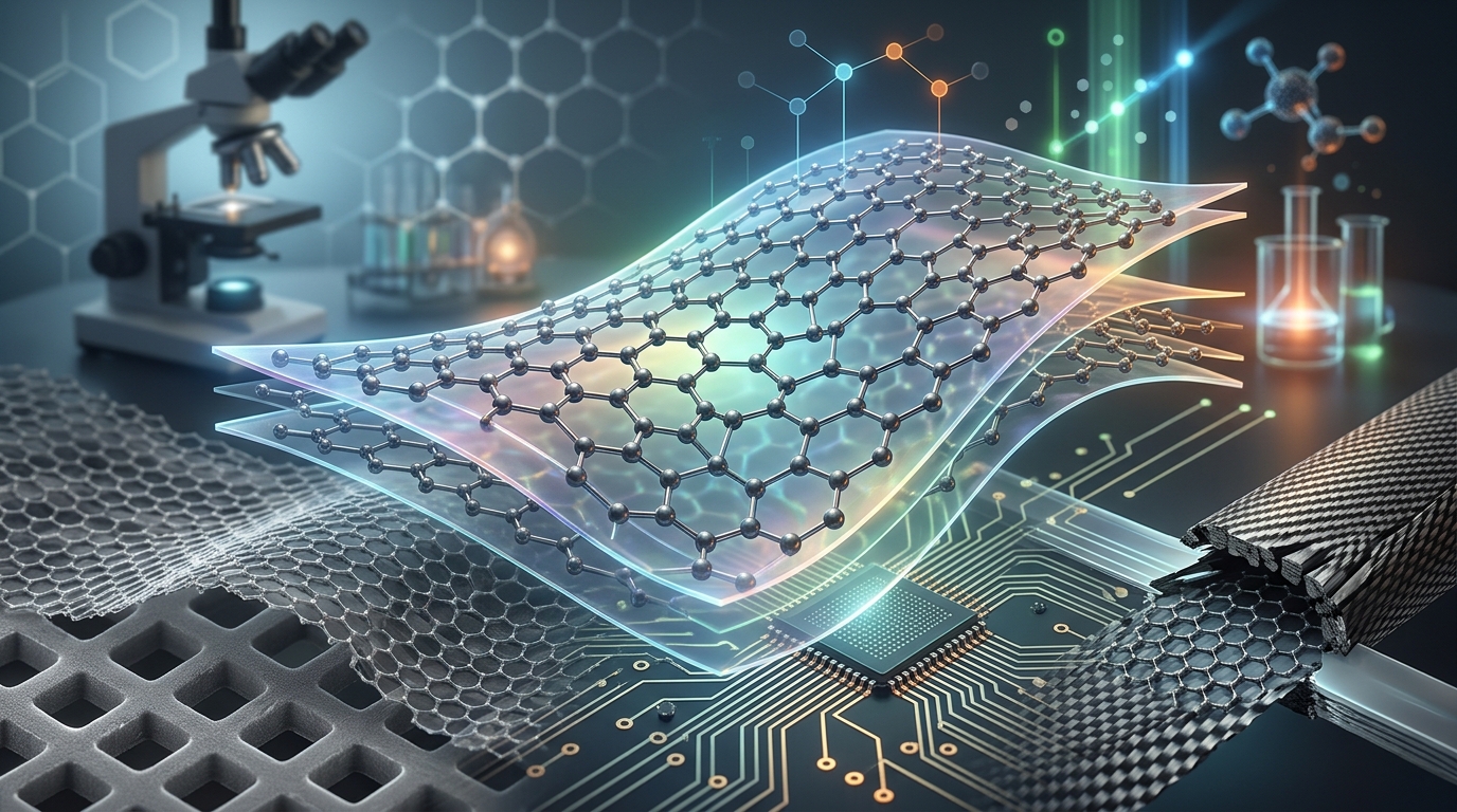
Graphene’s material properties align directly with specific functional requirements across multiple advanced technological domains:
- Thermal Management: Ultrahigh in-plane thermal conductivity provides efficient directional heat spreading for dense microelectronics, radio-frequency power amplifiers, and light-emitting diodes, mitigating localized thermal hotspots.
- High-Frequency Electronics: Exceptional carrier mobility and saturation velocity support analog, radio-frequency (RF), and terahertz field-effect transistors capable of operating at elevated cutoff frequencies, though logic applications remain limited by bandgap constraints.
- Optoelectronics and Photodetectors: Spectrally uniform optical absorption, ultrafast carrier recombination dynamics, and strong saturable absorption drive broadband, sub-picosecond photodetectors and optical modulators for high-bandwidth telecommunications.
- Barrier Coatings and Membranes: Complete helium impermeability combined with atomic thinness enables chemical anti-corrosion barriers, ultra-thin hermetic encapsulation layers for moisture-sensitive organic electronics, and engineered molecular-sieving membranes.
- Structural Nanocomposites: Superior intrinsic tensile strength and Young’s modulus allow low-fraction loading into polymers, metals, and ceramic matrices to enhance specific stiffness, structural fatigue resistance, and electrical conductivity.