Graphene Nanoribbons
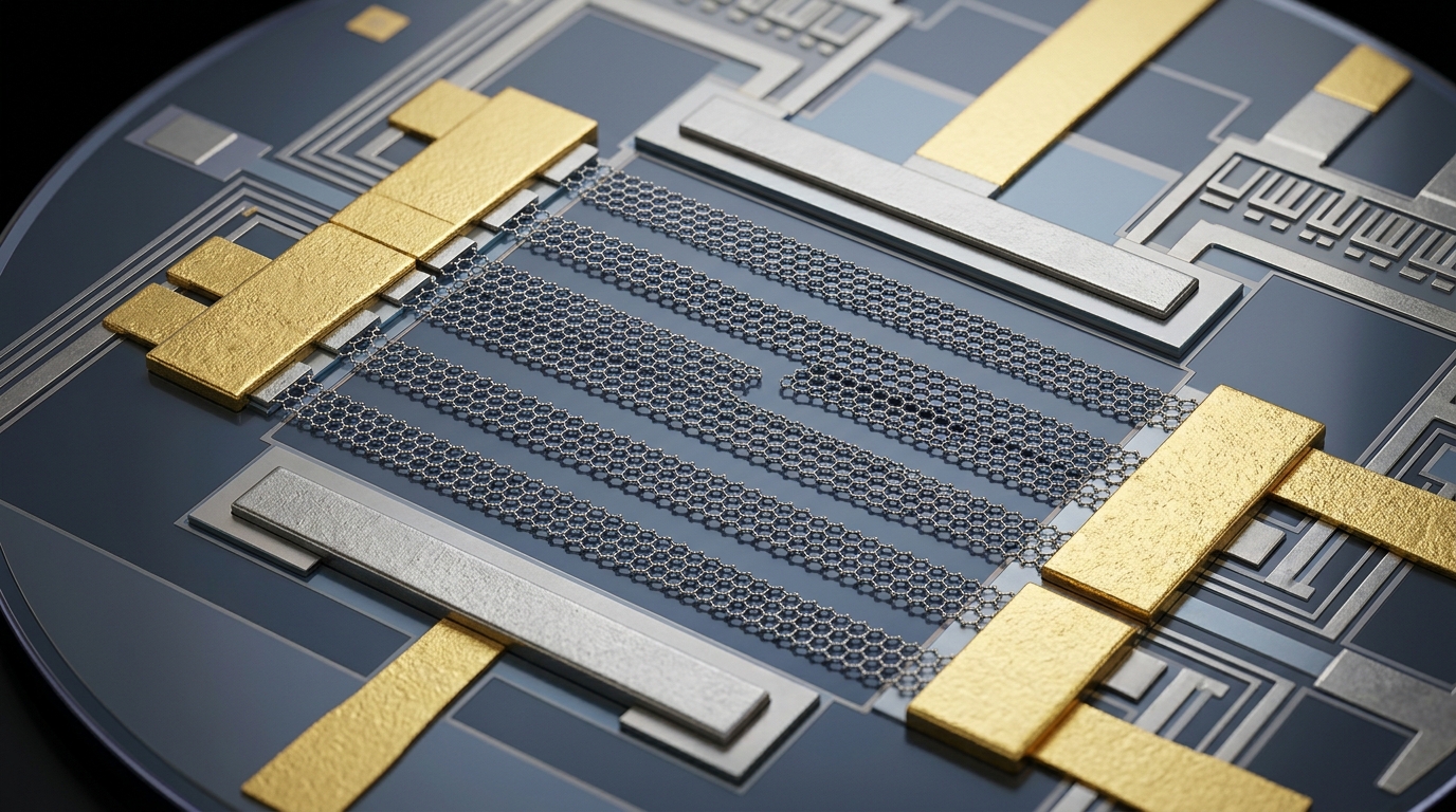
Graphene nanoribbons (GNRs) are quasi-one-dimensional strips of single-layer graphene characterized by finite lateral widths, typically below 50 nanometers, and high aspect ratios. While pristine two-dimensional graphene functions as a zero-bandgap semimetal with relativistic-like Dirac fermions, spatial lateral confinement restricts electron motion in the transverse direction. This geometric modification alters the low-energy electronic structure, inducing a finite bandgap that enables binary switching. Consequently, graphene nanoribbons are actively researched as viable channel materials for next-generation field-effect transistors, quantum components, and spintronic devices.
Quantum Confinement and Bandgap Opening
Pristine 2D graphene exhibits conical conduction and valence bands that meet at the Brillouin zone corners, designated as the Dirac ($K$ and $K’$) points. The absence of a fundamental bandgap prevents pristine 2D graphene from shutting off current in digital logic architectures, restricting its on/off current ratio ($I_{on}/I_{off}$) to single-digit values at room temperature. In digital electronics, switching logic requires clear distinctions between on and off states, typically necessitating an $I_{on}/I_{off}$ ratio of $10^4$ to $10^7$ along with a bandgap of at least 0.4 to 0.8 electronvolts (eV).
Confining the graphene sheet laterally into an elongated ribbon introduces hard-wall boundary conditions that quantize the transverse wave vector ($k_ot$). Rather than populating a continuous two-dimensional manifold, electronic states separate into discrete subbands. The energy spacing between these subbands—and the resulting energy bandgap ($E_g$)—is inversely related to the ribbon width ($w$):
$$E_g propto frac{hbar v_F}{w}$$
where $v_F approx 10^6text{ m/s}$ represents the Fermi velocity in graphene, and $hbar$ is the reduced Planck constant. To establish a bandgap sufficient for standard digital complementary metal-oxide-semiconductor (CMOS) logic operations at ambient temperatures ($E_g ge 0.5text{ eV}$), the ribbon width must be scaled below approximately 2 to 3 nanometers. At these atomic dimensions, the physical configuration of the ribbon termination—known as edge topology—critically governs the electronic dispersion.
Edge Topology: Armchair vs. Zigzag Configurations
The electronic band structure of a graphene nanoribbon depends directly on the crystallographic orientation of its edges. Depending on how the hexagonal carbon lattice is terminated, nanoribbons fall primarily into two symmetric categories: armchair graphene nanoribbons (AGNRs) and zigzag graphene nanoribbons (ZGNRs), alongside intermediate chiral geometries.
Armchair Graphene Nanoribbons (AGNRs)
Armchair edges are defined by an edge vector aligned parallel to the carbon-carbon bonds, forming a geometric profile resembling an armchair. The width of an AGNR is conventionally classified by the number of carbon dimer lines ($N$) across the ribbon width.
Based on tight-binding calculations with boundary constraints, AGNRs partition into three distinct structural families: $N = 3p$, $N = 3p + 1$, and $N = 3p + 2$, where $p$ is an integer:
- $N = 3p + 1$ Family: Possesses the largest bandgaps due to destructive quantum interference at the edge boundary. These structures are wide-gap semiconductors well suited for high-temperature switching.
- $N = 3p$ Family: Exhibits intermediate semiconductor bandgaps, scaling inversely with ribbon width.
- $N = 3p + 2$ Family: Simple zone-folding approximations predict metallic behavior for this hierarchy. However, second-nearest-neighbor hopping and self-consistent electron-electron interactions, coupled with bond-length contraction along the edges, break the valley degeneracy. This opens a finite, quasi-metallic direct bandgap on the order of tens to hundreds of millielectronvolts, retaining semiconducting behavior at physical sub-nanometer scales.
Because AGNRs yield non-zero direct bandgaps without intrinsic magnetic edge states, they serve as the primary focus for planar electrostatic field-effect transistor channels.
Zigzag Graphene Nanoribbons (ZGNRs)
Zigzag edges terminate parallel to the zigzag lines of the hexagonal lattice, with width indexed by the number of zigzag chains ($N_z$). The boundary condition in ZGNRs forces electrons into non-bonding $pi$-orbitals localized strictly at the peripheral carbon atoms. This structural arrangement produces flat electronic bands near the Fermi level, generating a high localized density of states (LDOS).
Because of strong intra-edge exchange interactions driven by Coulomb repulsion, the edge states undergo spontaneous spin polarization:
- Intra-edge Coupling: Spin states align ferromagnetically along a single edge.
- Inter-edge Coupling: Across the ribbon width, the two opposing edges couple antiferromagnetically in the ground state.
In its equilibrium ground state, a pristine ZGNR operates as an antiferromagnetic insulator or semiconductor with zero net magnetic moment. Applying a transverse in-plane electric field breaks this spatial inversion symmetry, shifting the electrostatic potential of the two edges in opposite directions. At a critical field threshold, the energy gap for one spin channel closes while the other remains wide, driving the ribbon into a half-metallic state. This distinct spin-split behavior makes ZGNRs compelling candidates for low-power spintronic devices.
Heteroatom Doping and Band Structure Modulation
Beyond dimensional confinement and crystallographic edge orientation, introducing heteroatoms into the hexagonal carbon lattice allows precise modulation of the electronic properties of graphene nanoribbons.
Incorporating boron (B) atoms—which possess one fewer valence electron than carbon—yields p-type acceptor states, shifting the ribbon Fermi level down toward the valence band. Conversely, substituting nitrogen (N) atoms supplies excess electrons, generating n-type donor states and shifting the Fermi level upward toward the conduction band. Spatially positioning alternating B-N pairs throughout the inner lattice or along the edges induces localized polar bonds that open wider electronic gaps without reducing physical ribbon widths. These heterojunctions and modulated segments enable the design of intra-ribbon p-n junctions, quantum dots, and resonant tunneling barriers within a single contiguous carbon framework.
Synthesis Routes: Top-Down vs. Bottom-Up
Synthesizing GNRs with controlled widths, uniform edge configurations, and minimal structural defects requires specialized processing routes. Fabrication methodologies are broadly categorized into top-down subtractive techniques and bottom-up additive chemical syntheses.
| Metric / Feature | Top-Down Approaches (Lithography, Unzipping) | Bottom-Up Approaches (On-Surface Chemical Synthesis) |
|---|---|---|
| Edge Control | Rough, disordered edge profiles with mixed AGNR/ZGNR segments | Atomically precise edge terminations |
| Width Distribution | Polydisperse; typically $>5text{ nm}$ (lithography) or variable (unzipping) | Strictly monodisperse, defined by organic precursor monomer structure |
| Bandgap Uniformity | Low; fluctuations caused by edge scattering and variable confinement | High; reproducible electronic gaps matching molecular predictions |
| Scalability | Compatible with standard semiconductor wafer integration | Constrained by ultra-high vacuum conditions and metallic growth substrates |
| Defect Density | Moderate to high (vacancies, functionalization from aggressive chemistry) | Negligible intrinsic lattice vacancies within the synthesized domains |
Top-Down Approaches
Top-down strategies sculpt ribbons out of broader graphite matrices, multi-walled carbon nanotubes, or continuous monolayer graphene:
- Lithographic Patterning: High-resolution electron-beam lithography (EBL), block-copolymer self-assembly, or scanning-probe lithography are used alongside oxygen or argon reactive ion etching (RIE) to carve narrow strips from large-area 2D graphene. While lithography allows precise spatial positioning on target substrates, it generally cannot scale below 5 nm without introducing substantial line-edge roughness. Irregular edge margins scatter charge carriers, degrading carrier mobility and obscuring edge-state phenomena.
- Carbon Nanotube Unzipping: Multi-walled or single-walled carbon nanotubes (CNTs) are sliced longitudinal-wise through oxidative acid treatments (e.g., potassium permanganate in sulfuric acid), catalytic metal particle cutting, or argon plasma etching. Oxidative unzipping yields ribbons with widths dictated by the parent nanotube diameter, but introduces high oxygen-defect densities, structural vacancies, and varied edge chiralities that require thermal annealing to partially repair.
Bottom-Up On-Surface Synthesis
Bottom-up synthesis utilizes organic chemistry to achieve atomic precision. Precursor molecules—carefully engineered aromatic hydrocarbons with halogen functional groups (such as brominated or iodinated bianthryl derivatives)—are deposited onto single-crystal metal surfaces (primarily Au(111), Ag(111), or Cu(111)) under ultra-high vacuum (UHV) conditions.
The reaction proceeds through a sequential, thermally activated mechanism:
- Dehalogenation and Polymerization: Heating the substrate to approximately 200°C activates carbon-halogen bond cleavage, generating surface-stabilized biradicals that couple via Ullmann-type reaction steps into extended linear polyanthrylene polymers.
- Cyclodehydrogenation: Further heating to approximately 400°C induces intramacromolecular cyclodehydrogenation. The intermediate polymers planarize through oxidative ring-closure, forming fully conjugated, atomically pristine armchair or zigzag graphene nanoribbons.
Bottom-up methods can also produce heterostructured GNRs with variable segments or heteroatomic dopants by using customized precursor molecules. However, the process yields finite ribbon lengths (typically 20 to 100 nm) on catalytic metal substrates, requiring clean transfer to insulating targets for device integration.
Device Applications: Transistors, Mobility, and Spintronics
The electronic and spin characteristics of graphene nanoribbons offer direct performance advantages across several high-density device paradigms.
Field-Effect Transistors (FETs)
Planar graphene field-effect transistors using wide, pristine 2D sheets cannot switch off completely, yielding insufficient static power dissipation for logic applications. In contrast, narrow AGNRs possess bandgaps exceeding 0.5 eV, providing low off-state leakage currents.
In field-effect transistors built with bottom-up-synthesized 9-atom wide AGNRs (9-AGNRs), researchers have demonstrated room-temperature $I_{on}/I_{off}$ switching ratios exceeding $10^5$, with theoretical subthreshold swings approaching the fundamental thermionic limit of 60 millivolts per decade (mV/dec). These switching profiles position sub-2 nm AGNRs as viable candidates for ultra-scaled logic nodes requiring high transconductance.
Carrier Mobility: GNRs vs. Silicon and TMDs
A critical consideration in solid-state devices is the balance between carrier mobility and the fundamental bandgap:
- Comparison to Silicon: Bulk silicon exhibits an electron mobility of approximately 1,400 $text{cm}^2/text{V}cdottext{s}$ at room temperature, which degrades below 500 $text{cm}^2/text{V}cdottext{s}$ in ultra-thin body configurations under 5 nanometers due to surface roughness and surface phonon scattering. In theoretical models of narrow AGNRs with clean edges, phonon-limited carrier mobility ranges from 1,000 to over 3,000 $text{cm}^2/text{V}cdottext{s}$ at equivalent bandgaps, providing potential drive-current advantages at scaled nodes.
- Comparison to Transition Metal Dichalcogenides (TMDs): Monolayer TMDs like molybdenum disulfide ($text{MoS}_2$) possess natural bandgaps between 1.5 and 2.0 eV, but display moderate room-temperature carrier mobilities (typically 20 to 100 $text{cm}^2/text{V}cdottext{s}$ on common substrates). Atomically precise GNRs combine comparable bandgaps with lower effective carrier masses, supporting higher saturation velocities and reduced channel transit times.
Experimentally realized GNR devices often display lower mobilities than theoretical upper limits, as edge defects, substrate impurities, and high contact resistances at metal interfaces cause real-world performance losses.
Spintronics and Edge-State Devices
Zigzag graphene nanoribbons provide a platform for carbon-based spintronics without requiring heavy rare-earth magnetic elements. Because spin-orbit coupling in carbon is naturally weak ($< 50 mutext{eV}$), electron spins maintain long spin lifetimes and diffusion lengths.
By using ferromagnetic electrodes to selectively inject spin-polarized currents, or by gating the opposing edges independently, ZGNR channels can serve as pure spin filters, spin-logic gates, and non-volatile magnetic memory cells. In these designs, logic states are represented by the spin orientation of the edge states rather than physical charge packets.
Manufacturing Bottlenecks and Integration Challenges
Despite their favorable theoretical physics, graphene nanoribbons face several structural and manufacturing challenges that hinder their integration into commercial electronics:
- Edge Precision Sensitivity: Deviations of a single carbon atom along the edge of a sub-2 nm ribbon disrupt local quantum confinement. A single edge defect or atomic vacancy can act as an elastic scattering site, converting semiconducting bands into localized defect states, causing resonant backscattering, and reducing carrier mobility by up to two orders of magnitude.
- Substrate Transfer and Contamination: The most consistent synthesis route—bottom-up on-surface coupling—takes place on metallic single crystals like Au(111). Integrating ribbons into transistors requires transferring these sub-nanometer-wide structures onto insulating dielectric substrates like $text{SiO}_2$, $text{Al}_2text{O}_3$, or hexagonal boron nitride (h-BN). Mechanical and chemical polymer-assisted transfer processes risk introducing folds, carbonaceous residues, mechanical strain, and chemical contamination that degrade ribbon-dielectric interfaces.
- Contact Resistance ($R_c$): Fabricating low-resistance, ohmic contacts to narrow-gap GNRs is challenging. Their small density of states and narrow cross-sectional areas establish high Schottky barrier heights with standard metal contacts (titanium, palladium, gold), which creates high parasitic contact resistance that limits maximum drive currents.
- Assembly Alignment and Spatial Scalability: Conventional synthesis routes produce randomly oriented networks of nanoribbons. Fabricating modern integrated circuits with billions of operational transistors requires unidirectional alignment, deterministic placement, uniform spatial spacing, and consistent channel lengths across 300 mm wafer targets.
Researchers are pursuing alternative approaches to resolve these constraints, including direct non-metallic on-surface synthesis on wide-bandgap insulators, seed-mediated template growth, and fluidic alignment strategies. The commercial viability of graphene nanoribbons depends on developing fabrication techniques that preserve atomic edge precision while providing the yield and reproducibility required for large-scale device integration.