CVD Graphene Films
CVD graphene films are continuous, large-area sheets of single- to few-layer carbon atoms synthesized via catalytic chemical vapor deposition. Unlike graphene powders or liquid-phase exfoliated flakes, which consist of discontinuous microscopic platelets suited for bulk composite additives, CVD films provide an unbroken, atom-thick planar architecture. This continuous sheet geometry makes them the standard material choice for transparent conductors, high-frequency electronics, photonic devices, barrier coatings, and sensitive biosensing channels.
The Fundamental Mechanism of CVD Graphene Growth
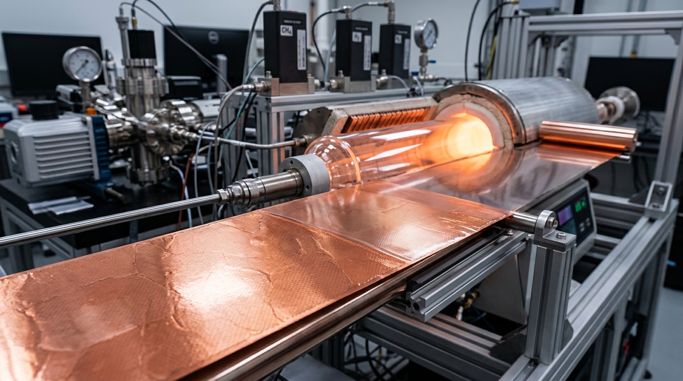
Chemical vapor deposition creates graphene by exposing a catalytic metal substrate to volatile carbon-containing precursor gases at elevated temperatures, typically between 800 and 1,050 degrees Celsius. The chemical dynamics of the reaction depend primarily on the catalytic substrate chosen, which dictates whether the growth is self-limiting or precipitation-driven.
Surface Catalysis on Copper Foils
Copper (Cu) is the most widely adopted catalyst for growing monolayer graphene films. Copper exhibits exceptionally low carbon solubility, meaning carbon atoms do not dissolve deeply into the bulk metal matrix at typical process temperatures. Instead, growth relies on a surface-mediated growth mechanism.
When a gaseous hydrocarbon precursor—most commonly methane (CH₄) mixed with hydrogen (H₂)—passes over heated copper foil, the catalytic metal surface cracks the hydrocarbon molecules into reactive carbon radicals (CHₓ). These carbon radicals diffuse across the copper surface, nucleate into microscopic crystalline islands (domains), and expand outward until they merge. Once the copper surface is completely covered by a single atomic sheet of carbon, the catalytic surface is shielded from incoming precursor gas. This effectively halts further decomposition, resulting in self-limiting single-layer growth with monolayer coverage frequently exceeding 95% of the substrate area.
Carbon Dissolution and Segregation on Nickel
In contrast to copper, nickel (Ni) has high carbon solubility at high temperatures. During the heating and exposure stage, carbon atoms dissolve rapidly into the bulk nickel foil. When the system cools, the solubility of carbon in nickel drops sharply, forcing excess carbon to precipitate and segregate out to the metal surface.
Because cooling rates and local grain orientations within the metal vary, carbon segregation on nickel tends to produce non-uniform films with varying thicknesses, ranging from single-layer regions to multi-layer patches and thicker graphite flakes. Consequently, nickel is rarely used when uniform monolayer films are required, though it remains useful for specialized applications requiring thicker, robust few-layer graphene films.
Low-Pressure vs. Atmospheric-Pressure Growth
The operational pressure inside the reactor directly shapes the nucleation density and domain size of the resulting film:
- Low-Pressure CVD (LPCVD): Conducted at pressures ranging from a few millitorr to several torr. LPCVD reduces the concentration of active carbon species in the boundary layer above the catalyst, suppressing excessive nucleation. This lower nucleation density encourages the growth of larger individual single-crystal domains before coalescence.
- Atmospheric-Pressure CVD (APCVD): Conducted at ambient pressure using inert carrier gases like argon. APCVD provides higher mass transport rates and faster growth cycles, but the higher concentration of reactive radicals can lead to higher nucleation density, smaller grain sizes, and potential multi-layer formation if gas flow ratios are not precisely calibrated.
Film Morphology and the Impact of Grain Boundaries
A standard CVD graphene film is not a single flawless crystal across its entire macro-scale area; it is a polycrystalline fabric composed of millions of intergrown single-crystal domains. The interfaces where these expanding domains collide and stitch together are known as grain boundaries.
Grain boundaries consist of alternating topological defects, such as pentagon-heptagon carbon rings (Stone-Wales defects), out-of-plane ripples, and misaligned crystal lattices. These boundaries govern several core performance attributes:
- Electrical Scattering: Grain boundaries act as potential barriers that disrupt ballistic electron transport, reducing effective carrier mobility compared to pristine, mechanically exfoliated flakes.
- Chemical Reactivity: The strained bonds at grain boundaries exhibit higher chemical reactivity, making them preferential sites for functionalization, oxidation, and unwanted environmental degradation.
- Mechanical Strength: While individual graphene domains exhibit the theoretical intrinsic breaking strength of $130 ext{ GPa}$, polycrystalline CVD films fail at lower stresses because mechanical fracture typically nucleates along misaligned domain interfaces.
- Barrier Impermeability: Atomic vacancies and micro-voids along poorly stitched boundaries can allow tiny gas molecules, such as helium or hydrogen, to permeate through an otherwise impermeable 2D lattice.
To mitigate these limitations, growth protocols often optimize hydrogen partial pressure, utilize electropolished single-crystal copper foils (such as Cu(111)), or introduce trace oxygen to passivate nucleation sites, allowing individual single-crystal domains to grow to millimeter or centimeter scales before merging.
The Substrate Transfer Process
Because CVD graphene is synthesized on metallic catalysts, it must be separated from the metal and transferred onto an insulating, transparent, or flexible target substrate—such as silicon dioxide (SiO₂), quartz, polyethylene terephthalate (PET), or glass—to be used in electronic or optical devices. The transfer process is often the most challenging stage in manufacturing, as it introduces defects, mechanical tears, and chemical residues.
Polymer-Assisted Wet Transfer
The standard laboratory and small-batch production technique uses a sacrificial polymer support layer, typically poly(methyl methacrylate) (PMMA):
- A thin layer of PMMA is spin-coated over the graphene-covered copper foil and cured.
- The underlying copper substrate is chemically etched away using an aqueous etchant solution, such as ferric chloride (FeCl₃) or ammonium persulfate ((NH₄)₂S₂O₈).
- The floating PMMA/graphene membrane is rinsed multiple times in deionized water baths to remove residual etchant salts.
- The floating stack is scooped onto the target substrate and dried.
- The PMMA scaffold is dissolved using organic solvents, such as acetone, followed by thermal annealing.
While straightforward, wet transfer leaves microscopic polymer residues and solvent stains that degrade carrier mobility and increase surface roughness. Additionally, capillary forces during drying can introduce wrinkles and micro-cracks.
Roll-to-Roll and Dry Delamination
For industrial-scale manufacturing, continuous roll-to-roll transfer systems replace wet batch chemical etching. In a roll-to-roll configuration, flexible target films coated with thermal-release tape or curable adhesive polymers are laminated directly against the graphene-on-copper web.
The graphene is then mechanically peeled away from the metal substrate—frequently assisted by electrochemical bubbling, where hydrogen gas generated at the metal-graphene interface gently lifts the carbon sheet without consuming the expensive copper foil. The metal foil can then be reconditioned and reused, substantially lowering industrial production costs.
Key Material Properties and Realistic Benchmarks
The physical properties of CVD graphene films depend heavily on layer count, transfer quality, and post-processing cleanliness. The table below illustrates the performance characteristics of high-quality transferred CVD monolayer films alongside theoretical pristine limits:
| Property | Theoretical Single-Crystal Monolayer | Typical Transferred CVD Monolayer Film |
|---|---|---|
| Optical Transmittance (at $550 ext{ nm}$) | 97.7% | 96.5% – 97.5% |
| Carrier Mobility (Room Temp.) | > $200,000 ext{ cm}^2/( ext{V} imes ext{s})$ | $1,000 ext{ – }5,000 ext{ cm}^2/( ext{V} imes ext{s})$ (on $ ext{SiO}_2$) > $20,000 ext{ cm}^2/( ext{V} imes ext{s})$ (encapsulated in h-BN) |
| Intrinsic Sheet Resistance (Undoped) | ~ $6,000 ext{ } ext{Ω/sq}$ (at Dirac point) | $300 ext{ – }1,500 ext{ } ext{Ω/sq}$ (ambient p-doped) |
| Sheet Resistance (Chemically Doped) | N/A | $30 ext{ – }150 ext{ } ext{Ω/sq}$ (with $ ext{HNO}_3$, $ ext{AuCl}_3$, or polymer dopants) |
| Young's Modulus | ~ $1.0 ext{ TPa}$ | $0.7 ext{ – }0.95 ext{ TPa}$ |
Practical and Industrial Applications
Transparent Conductive Electrodes (TCEs)
Indium Tin Oxide (ITO) is the conventional standard for transparent conductors in displays, but it is brittle, expensive, and prone to micro-cracking when flexed. CVD graphene films provide high optical transparency (~97.7% per layer) coupled with mechanical elasticity, tolerating repeated bending cycles without loss of conductivity. To match the low sheet resistance of ITO (typically 10 to 30 $ ext{Ω/sq}$), multi-layer CVD stacks combined with non-volatile chemical dopants (such as nitric acid, metal chlorides, or conductive polymers) are employed in capacitive touchscreens, organic light-emitting diodes (OLEDs), and flexible solar cells.
Field-Effect Transistors and High-Frequency Electronics
Because graphene has no intrinsic bandgap, standard CVD graphene cannot be completely switched off in logic circuits, making it unsuitable for direct replacement of silicon in digital microprocessors. However, its exceptional carrier velocity and ambipolar transport make it an outstanding candidate for analog radio-frequency (RF) communications, terahertz detectors, and field-effect transistors (FETs) where high operating frequencies and high cut-off limits ($f_T$) are paramount.
Biosensors and Diagnostic Chips
In a monolayer CVD film, every single atom is directly exposed to the surrounding environment. When target molecules bind to the functionalized surface of a graphene channel in a liquid-gated field-effect biosensor, the resulting charge redistribution induces immediate, measurable shifts in channel conductivity. CVD films enable wafer-scale fabrication of uniform diagnostic arrays capable of detecting single-molecule interactions, DNA hybridization, protein biomarkers, and pathogen presence at picomolar or femtomolar concentrations.
Ultra-Thin Barrier and Anti-Corrosion Layers
The dense, overlapping electron clouds within the hexagonal carbon rings create an impenetrable energy barrier to all atoms and molecules under ambient conditions. CVD graphene films transferred onto vulnerable metals serve as ultra-thin passivation coatings that prevent atmospheric oxidation and galvanic corrosion without altering the base metal’s dimensions or thermal dissipation profile. Similarly, defect-free CVD films act as impermeable membranes in specialized gas separation and ultra-high-vacuum systems.
Characterization and Quality Assessment
Assessing the quality, thickness, and structural integrity of CVD graphene films requires complementary non-destructive and analytical metrology tools:
- Raman Spectroscopy: The primary non-destructive characterization standard. A high-quality pristine monolayer is identified by a sharp, symmetric $2 ext{D}$ band at $ ext{~}2680 ext{ cm}^{-1}$ with an intensity ratio ($I_{2D}/I_G$) greater than 2, and a negligible defect-induced $ ext{D}$ band at $ ext{~}1350 ext{ cm}^{-1}$. The intensity ratio $I_D/I_G$ directly quantifies the density of structural defects and edge disorder.
- Atomic Force Microscopy (AFM): Evaluates topographic uniformity, confirms single-layer step heights ($ ext{~}0.4 ext{ to }0.7 ext{ nm}$ on target substrates due to surface interactions), and maps out transfer-induced wrinkles, tears, or polymer residues.
- Scanning Electron Microscopy (SEM): Provides fast, large-area imaging of domain morphology, allowing engineers to visualize coverage percentage, copper grain structures, and second-layer nucleation patches prior to transfer.
- Non-Contact Eddy Current and Four-Point Probe Mapping: Measures sheet resistance and electrical spatial uniformity across full wafers or rolls, identifying macroscopic fractures and doping uniformity without damaging the fragile atomic layer.
Material Selection and Integration Considerations
When selecting CVD graphene films for research or device manufacturing, several practical tradeoffs must be evaluated:
- Monolayer vs. Multi-layer: Monolayer films provide maximum optical transmission and field-effect sensitivity. Multi-layer films (often fabricated by sequential layer transfers) provide lower sheet resistance and greater fault tolerance against pinhole defects for barrier and electromagnetic shielding applications.
- Substrate Surface Chemistry: Polar substrates with high surface roughness or dangling bonds, such as untreated silicon dioxide, induce charge-carrier scattering and degrade mobility. Incorporating an atomically smooth buffer layer, such as hexagonal boron nitride (h-BN), preserves the intrinsic transport properties of the CVD film.
- Doping Stability: While chemical doping dramatically reduces sheet resistance, volatile dopants desorb over time or degrade when exposed to heat and moisture. Commercial implementations require barrier passivation coatings (such as thin atomic layer deposition alumina, $ ext{Al}_2 ext{O}_3$) to lock in electrical performance over long product lifespans.