CVD Graphene Films
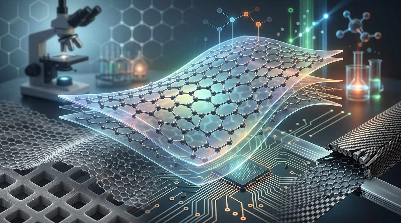
Chemical vapor deposition (CVD) graphene films represent the primary technological pathway for synthesizing large-area, continuous, high-crystallinity graphene sheets on a scalable substrate. Unlike liquid-phase exfoliation, which yields small, discontinuous flakes, CVD enables the bottom-up growth of wafer-scale and roll-to-roll monolayer and few-layer films. These continuous two-dimensional sheets preserve the fundamental optoelectronic properties of graphene—including high theoretical carrier mobility, broadband optical transparency (~97.7% per monolayer), and exceptional mechanical flexibility—making them the standard format for integration into advanced electronics, photonics, and transparent electrodes.
Fundamentals of CVD Graphene Synthesis
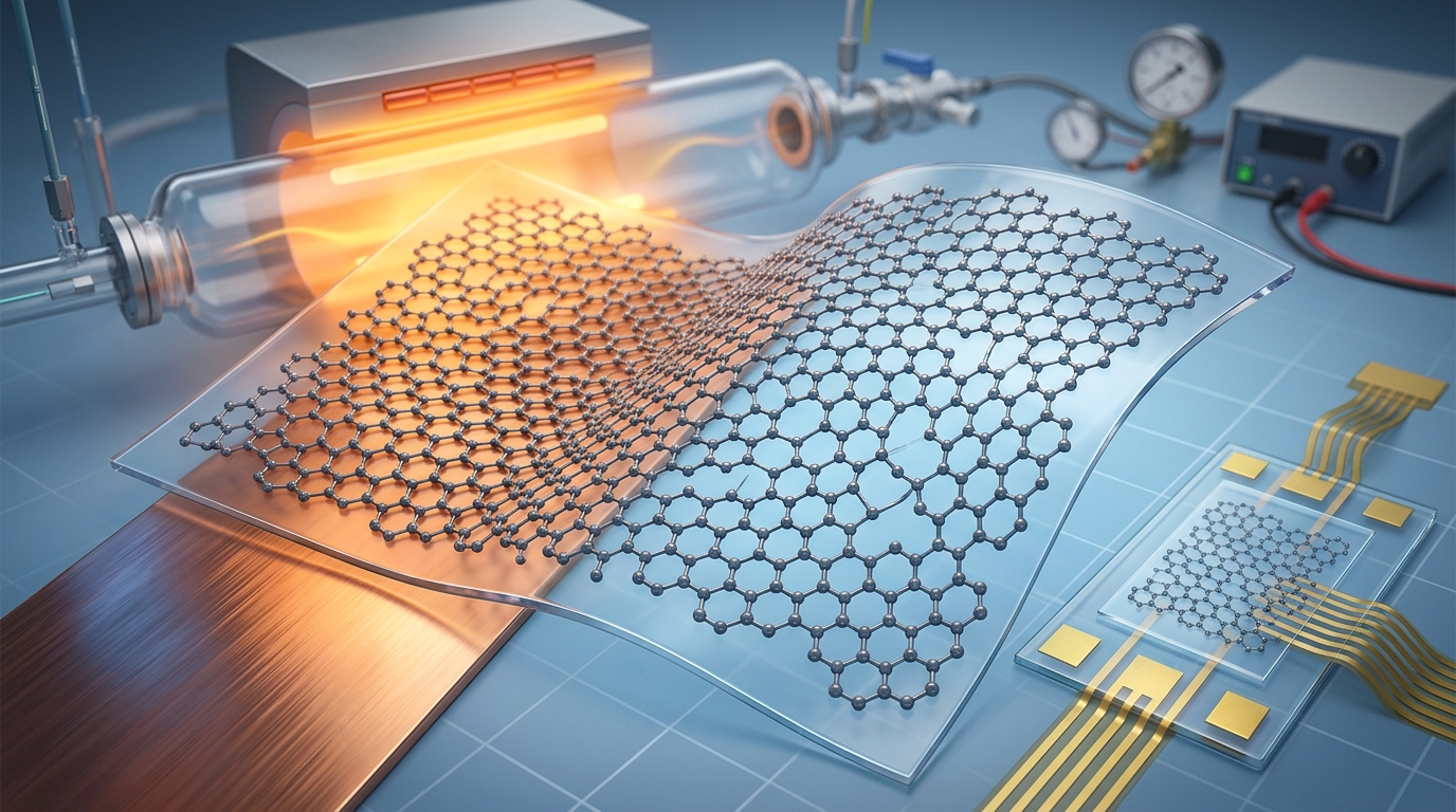
The synthesis of CVD graphene relies on the catalytic decomposition of a carbonaceous precursor gas over a transition metal substrate at elevated temperatures, typically between 800°C and 1050°C. The choice of catalyst metal dictates whether the growth follows a surface-mediated or segregation-precipitation mechanism, which directly impacts layer uniformity, grain size, and defect density.
Catalyst Mechanisms: Copper vs. Nickel
The two most widely studied catalyst substrates are copper (Cu) and nickel (Ni), each exhibiting distinct carbon solubilities and growth kinetics:
- Copper (Cu) – Surface-Mediated Growth: Copper has an exceptionally low carbon solubility (<0.001 atom% at 1000°C). When a hydrocarbon precursor such as methane (CH4) dissociates on the copper surface, carbon atoms do not dissolve significantly into the bulk metal. Instead, growth is surface-limited: once a complete monolayer covers the copper surface, the catalytic decomposition of methane ceases or slows dramatically. This self-limiting mechanism makes copper foils the industry standard for producing uniform, high-coverage monolayer graphene films.
- Nickel (Ni) – Dissolution-Segregation Growth: Nickel exhibits high carbon solubility (>0.1 atom% at 1000°C). At growth temperatures, carbon atoms rapidly dissolve into the bulk Ni substrate. Upon cooling, the solubility decreases sharply, forcing dissolved carbon to segregate and precipitate out onto the surface. Because precipitation rates vary across grain boundaries and crystallographic orientations of the metal, growth on nickel typically produces inhomogeneous, multilayer graphene films with variable thickness.
Process Parameters and Precursor Gases
The standard CVD recipe balances several process variables to control domain nucleation density and domain growth rate:
- Carbon Precursors: Methane (CH4) is the most common precursor due to its thermal stability and predictable dissociation kinetics. Liquid hydrocarbons (e.g., ethanol, benzene) or solid precursors (e.g., polymers) are occasionally used for low-temperature or specialized growth regimes.
- Hydrogen (H2) Role: Hydrogen acts as both a co-catalyst that activates C–H bond cleavage and an etchant that preferentially removes disordered carbon and etched weak C–C bonds, controlling the shape and edge termination of growing graphene domains.
- Pressure Regimes: Growth is conducted either under Low-Pressure CVD (LPCVD, typically 0.1 to 10 Torr) or Atmospheric-Pressure CVD (APCVD). LPCVD reduces gas-phase boundary layer resistance, promoting uniform nucleation across large foil areas, whereas APCVD enables faster growth rates and open-atmosphere roll-to-roll implementations.
Layer Number Control: Monolayer, Bilayer, and Multilayer CVD Films
Controlling the thickness and stacking order of CVD graphene determines its band structure, sheet resistance, and optical transmission.
| Film Classification | Typical Layer Count | Optical Transmission (~550 nm) | Theoretical Bandgap | Typical Sheet Resistance (Undoped) |
|---|---|---|---|---|
| Monolayer | 1 | ~97.7% | Zero bandgap (Dirac semi-metal) | 400 – 1500 Ω/sq |
| AB-Stacked Bilayer | 2 | ~95.4% | Tunable via vertical electric field | 250 – 800 Ω/sq |
| Turbostratic / Multilayer | 3 – 10 | 85% – 93% | Semimetallic / Screened | 50 – 300 Ω/sq |
Monolayer CVD Films
Synthesized predominantly on low-roughness copper foils, monolayer CVD graphene forms as individual hexagonal domains nucleate and coalesce into a continuous, polycrystalline film. Monolayer films exhibit the highest carrier mobility and transparency, serving as the benchmark for optoelectronic devices and fundamental transport studies.
Bilayer and Multilayer Formations
Bilayer CVD films can grow in Bernal (AB) stacking or twisted (non-Bernal) configurations. AB-stacked bilayers are particularly significant for field-effect transistor (FET) architectures because a perpendicular electrostatic displacement field can break inversion symmetry, opening a tunable bandgap up to approximately 250 meV. Multilayer films, often synthesized via high methane partial pressures or on catalytic alloys (such as Cu-Ni solutions), offer reduced sheet resistance by providing multiple parallel conduction channels, which is advantageous in transparent electrode applications where raw conductivity outranks extreme optical transmission.
Film Transfer Methodologies to Target Substrates
Because CVD graphene is grown on catalytic metal foils, it must be detached and transferred onto dielectric (e.g., SiO2/Si, quartz, glass) or flexible polymeric substrates (e.g., PET, PI) without introducing tears, wrinkles, or chemical contamination.
1. Wet Chemical Transfer (Polymer-Assisted)
Wet chemical transfer remains the most common laboratory and small-scale fabrication technique:
- Polymer Coating: A sacrificial supportive layer, most commonly poly(methyl methacrylate) (PMMA), is spin-coated onto the top surface of the graphene/copper foil.
- Substrate Etching: The underlying copper is chemically dissolved in an etchant bath, typically aqueous ferric chloride (FeCl3), ammonium persulfate ((NH4)2S2O8), or copper chloride (CuCl2).
- Rinsing: The free-floating PMMA/graphene membrane is transferred through multiple deionized (DI) water rinse baths to dilute residual etchant ions.
- Target Placement & Dissolution: The membrane is scooped onto the target substrate, dried to promote interfacial adhesion, and the PMMA layer is dissolved using organic solvents such as acetone or removed via thermal annealing.
2. Dry Transfer and Roll-to-Roll (R2R) Lamination
For flexible substrates, dry transfer minimizes chemical exposure. Thermal Release Tape (TRT) or a target adhesive polymer (such as EVA/PET) is laminated directly onto the CVD graphene on Cu foil. The metal foil is then chemically etched or mechanically delaminated. In the case of TRT, heating the stack to the tape’s release temperature cleanly releases the graphene onto the receiving substrate. Continuous roll-to-roll (R2R) setups leverage this method to produce continuous meters of graphene-on-PET films for industrial applications.
3. Polymer-Free and Electrochemical Delamination Transfer
To avoid metal-etching waste and polymer residues, electrochemical bubbling transfer uses the graphene/metal foil as a cathode in an aqueous electrolyte (e.g., NaOH or K2SO4). When a voltage is applied, hydrogen gas bubbles evolve at the graphene-metal interface, mechanically cleaving the graphene film from the metal without dissolving the copper. This allows the host metal foil to be cleaned and reused for subsequent CVD growth cycles.
Characterization Techniques for CVD Films
Assessing the structural integrity, continuity, and electronic properties of CVD graphene films requires complementary analytical tools:
- Raman Spectroscopy: The primary non-destructive standard for analyzing layer count, defect density, and strain. The spectra exhibit three primary peaks: the D peak (~1350 cm-1), representing symmetry-breaking defects and grain boundaries; the G peak (~1580 cm-1), representing in-plane sp2 C–C stretching; and the 2D peak (~2690 cm-1), the second-order overtone of the D peak. A pristine monolayer on SiO2 is characterized by a symmetric 2D peak with a Full Width at Half Maximum (FWHM) ≤ 30 cm-1, an intensity ratio I2D/IG > 2, and a negligible D peak (ID/IG ≈ 0).
- Four-Point Probe & Hall Effect Measurements: Used to measure sheet resistance (Rs), carrier density, and carrier mobility (μ) across large-area films, identifying uniformity gradients and electrical bottlenecks caused by domain boundaries.
- Atomic Force Microscopy (AFM): Evaluates nanoscale surface topography, film thickness, step heights, and the presence of wrinkles or transfer residues.
CVD Films vs. Epitaxial Graphene on Silicon Carbide (SiC)
While CVD is the dominant method for versatile, transferrable films, epitaxial growth on silicon carbide (SiC) represents a key alternative approach in high-frequency electronics.
| Parameter | CVD Graphene Films | Epitaxial Graphene on SiC |
|---|---|---|
| Growth Substrate | Catalytic metals (Cu, Ni, Cu-Ni alloys) | Single-crystal Silicon Carbide (SiC) wafers |
| Transfer Requirement | Mandatory for non-metallic targets | None (grown directly on semi-insulating SiC) |
| Substrate Scalability | Roll-to-roll meters; arbitrary substrate transfer | Limited by SiC wafer diameter (e.g., 100–150 mm) |
| Substrate Cost | Low to moderate (reusable or thin foils) | Very high (single-crystal SiC wafers) |
| Primary Target Sector | Flexible devices, sensors, TCEs, general electronics | Ultra-high-frequency RF electronics, quantum metrology |
Key Industrial and Technological Applications
CVD graphene films provide unique multifunctionality where high electrical conductivity, optical transparency, and mechanical elasticity must coexist.
Transparent Conductive Electrodes (TCEs)
Indium tin oxide (ITO) is the commercial standard for transparent electrodes, but its brittleness limits its use in flexible displays, and indium supply constraints raise long-term cost concerns. CVD graphene films—frequently chemical-doped (e.g., with HNO3, AuCl3, or conductive polymers) to achieve sheet resistances below 100 Ω/sq while maintaining >90% transparency—serve as flexible transparent electrodes for organic photovoltaics (OPVs), organic light-emitting diodes (OLEDs), and capacitive touchscreens.
Flexible, Wearable, and Bio-Integrated Electronics
Because monolayer CVD graphene can withstand mechanical strains exceeding 10% without catastrophic electrical failure, it is uniquely suited for wearable interconnects, epidermal electronic tattoos, and flexible heating elements. When transferred onto biocompatible elastomers (such as PDMS or parylene), CVD films establish low-impedance, conformal bio-interfaces for recording electrophysiological signals (e.g., ECG, EEG, EMG) without skin irritation.
Radio Frequency (RF) and Field-Effect Devices
The high room-temperature field-effect mobility of transferred CVD films (often exceeding 3,000 to 10,000 cm2/(V·s) on typical dielectric substrates, and >50,000 cm2/(V·s) when encapsulated in hexagonal boron nitride) enables high-cutoff-frequency (>100 GHz) RF transistors, flexible frequency multipliers, and photodetectors covering spectral ranges from ultraviolet to terahertz.
Chemical and Biosensing Platforms
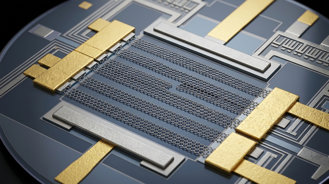
Because every carbon atom in a monolayer CVD film is directly exposed to the external environment, its surface conductivity is sensitive to electrostatic perturbation, molecular adsorption, and charge transfer. CVD graphene field-effect transistors (gFETs) functionalized with specific aptamers, antibodies, or catalytic nanoparticles serve as real-time, label-free sensors capable of detecting low-concentration biomolecules, hazardous gases (such as NO2 and NH3), and heavy metal ions in aqueous solutions.
Technological Bottlenecks and Quality Limitations
Despite commercial scale-up, several fundamental and engineering challenges continue to limit the performance of CVD graphene films relative to theoretical single-crystal values:
1. Polycrystallinity and Grain Boundaries
Standard CVD films are polycrystalline, formed by the coalescence of millions of randomly oriented graphene domains. The resulting grain boundaries consist of pentagon-heptagon defect pairs (disclinations and dislocations) that act as carrier scattering centers, reducing overall electrical mobility and mechanical tensile strength relative to single-crystal graphene.
2. Wrinkle Formation and Thermal Stress
During the post-growth cool-down phase, the mismatch between the thermal expansion coefficient of graphene (which is negative at low-to-moderate temperatures) and the underlying copper catalyst (positive, ~16 × 10-6 K-1) induces substantial compressive stress. This mismatch relieves itself through the formation of nanoscale wrinkles, which introduce localized strain, disrupt planar dielectric contact, and create preferential paths for current scattering.
3. Transfer-Induced Defects and Residues
Wet transfer processes routinely leave nanometer-scale residues of sacrificial polymer (e.g., PMMA) firmly adsorbed onto the graphene surface via π-π or van der Waals interactions. These organic residues cause uncontrolled p-type doping, increase surface roughness, and degrade mobility. Additionally, mechanical handling during transfer can introduce micro-cracks, pinholes, and trapped water or air pockets between the graphene and the target substrate.
4. Sheet Resistance Variations and Doping Instability
While pristine monolayer CVD graphene has an intrinsic sheet resistance of ~1000 Ω/sq, transparent electrode applications demand values <50 Ω/sq. Achieving these targets requires intentional chemical doping (intercalation or surface adsorption). However, many standard dopants (such as nitric acid) desorb or degrade under ambient thermal exposure, leading to progressive sheet resistance drift over time unless hermetically encapsulated.