Graphene vs. Graphite
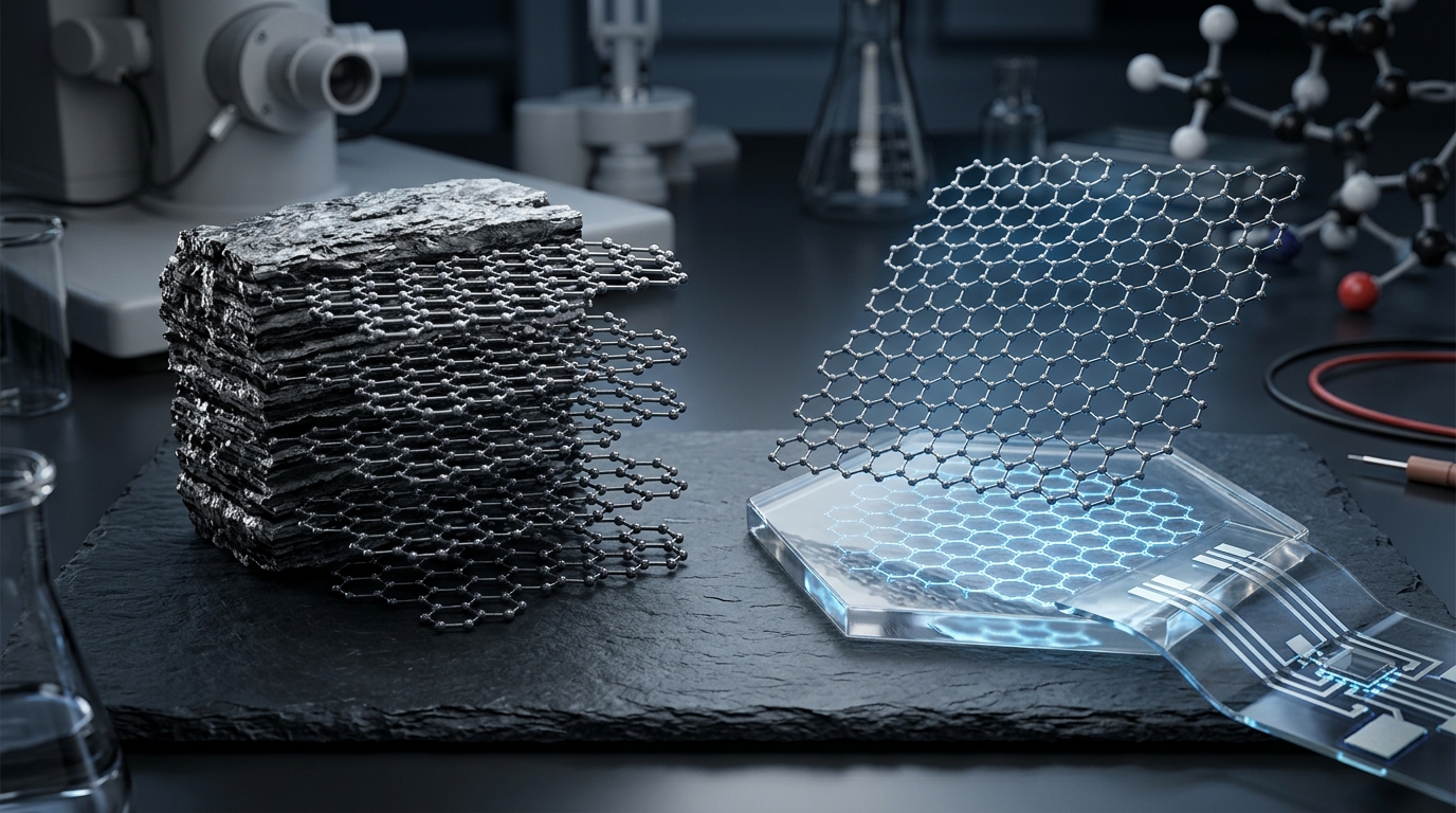
At the atomic scale, graphene and graphite are built from the exact same chemical foundation: pure carbon atoms bound tightly in a hexagonal, honeycomb lattice. The difference between them comes down to a single dimension. Graphene is a single two-dimensional sheet of carbon atoms, measuring just one atom thick. Graphite is the three-dimensional, bulk form of this material, consisting of millions of individual graphene sheets stacked on top of one another.
While graphite has been utilized for centuries in pencils, lubricants, and metallurgy, isolating a single graphene layer reveals physics that do not exist in the bulk mineral. Understanding graphene vs graphite requires examining how peeling apart stacked layers fundamentally alters mechanical durability, electrical behavior, heat transfer, and optical transparency.
Atomic Architecture: 2D Monolayer vs. 3D Stacked Lattice
Both allotropes rely on sp² hybridization. In this orbital arrangement, each carbon atom bonds covalently to three neighboring carbon atoms within the same plane at 120-degree angles. This arrangement creates exceptionally short, robust carbon-carbon bonds (approximately 0.142 nanometers) that form the classic planar honeycomb pattern.
The structural divergence occurs entirely in the third dimension:
- Graphene possesses no third dimension beyond its single atomic thickness of roughly 0.335 nanometers. Every atom is an exposed surface atom, making it an entirely two-dimensional crystal.
- Graphite features sheets stacked parallel to one another. While the in-plane bonds are among the strongest in nature, adjacent layers are held together only by weak van der Waals forces. The interlayer spacing between stacked planes measures approximately 0.335 nanometers, allowing layers to slide across one another under modest shear stress.
Property Comparison: How Stacking Alters Physics
When graphene sheets stack to form graphite, the electronic wavefunctions of adjacent layers overlap. This coupling dampens or entirely cancels many of the quantum phenomena observed in an isolated sheet.
Mechanical Strength vs. Natural Lubricity
An isolated monolayer of pristine graphene exhibits an intrinsic tensile strength of 130 gigapascals and an elastic modulus of 1 terapascal. Defect-free graphene can withstand enormous stretching force relative to its cross-sectional area because any applied load directly stresses primary covalent bonds across the plane.
Graphite exhibits high compressive and in-plane strength on microscopic scales, but bulk graphite fractures easily under tension and shears under gentle mechanical stress. Because the van der Waals interactions between layers are weak, the sheets slide apart easily. This interlayer slippage makes graphite an exceptional dry solid lubricant, but it prevents bulk graphite from matching graphene’s structural reinforcement capabilities.
Electrical and Electronic Behavior
Graphene is a zero-bandgap semimetal where charge carriers (electrons and holes) behave as massless Dirac fermions. Electrons travel through pristine graphene with minimal scattering, enabling ballistic electron transport at room temperature and electron mobility values exceeding 200,000 cm²/V·s under ideal laboratory conditions.
In graphite, the overlapping electronic states of stacked layers transform the material into a conventional semimetal. Electrical conductivity remains high along the planar directions (basal planes) but drops by several orders of magnitude perpendicular to the sheets (c-axis). The charge carrier mobility in graphite typically ranges from 10,000 to 20,000 cm²/V·s at room temperature.
Thermal Conduction
Heat in carbon materials travels primarily via acoustic vibrations called phonons. In pristine monolayer graphene, unobstructed thermal phonon propagation allows in-plane thermal conductivities between 3,000 and 5,000 W/m·K. In graphite, cross-plane phonon scattering limits bulk thermal conductivity to roughly 1,500 to 2,000 W/m·K along the basal plane, and down to less than 10 W/m·K across the stacked layers.
Optical Transparency
Graphite is completely opaque, absorbing all visible light within a few dozen atomic layers and reflecting light with a characteristic metallic, grayish-black luster. By contrast, single-layer graphene absorbs only 2.3% of incident white light, making it virtually transparent to the naked eye while retaining electrical continuity.
Technical Comparison Table
| Property / Metric | Monolayer Graphene | Natural / Synthetic Graphite |
|---|---|---|
| Dimensionality | Two-dimensional (2D) | Three-dimensional (3D bulk) |
| Layer Thickness | 1 carbon atom (~0.335 nm) | Thousands to billions of layers (>100 nm) |
| Tensile Strength | ~130 GPa (intrinsic, monolayer) | 4.8 to 15 MPa (bulk commercial) |
| Theoretical Surface Area | ~2,630 m²/g | Typically 1 to 20 m²/g |
| Optical Transmittance | ~97.7% visible light | 0% (Opaque black) |
| Carrier Mobility | Up to 200,000+ cm²/V·s (suspended) | ~10,000–20,000 cm²/V·s (in-plane) |
| Primary Interlayer Bonding | None (single plane) | Weak van der Waals forces |
The Classification Boundary: When Does Graphite Become Graphene?
A common point of confusion in materials science is the threshold separating thick graphene from thin graphite. International standards organizations (including ISO) have established formal conventions to classify these carbon forms:
- Monolayer Graphene: Exactly one layer of sp²-bonded carbon.
- Bilayer and Few-Layer Graphene (FLG): Stacks containing 2 to 10 distinct carbon layers. Within this range, quantum confinement effects and distinctive layer-dependent electronic properties remain observable.
- Graphene Nanoplatelets (GNPs): Particles with a thickness between 1 and 100 nanometers (up to roughly 300 layers), retaining platelet geometry with high aspect ratios.
- Graphite: Any carbon structure with more than the ten-layer boundary where bulk electronic band structures fully dominate and single-layer physics disappear.
Manufacturing and Processing: The Material Connection
Graphite is not just an alternative to graphene; it is the primary raw precursor from which most commercial graphene is derived. Processing methods dictate which material an engineer receives and the associated production economics.
Top-Down Exfoliation
The mechanical isolation of graphene in 2004 relied on micromechanical cleavage (the Scotch tape method), physically pulling graphene sheets away from bulk graphite. Modern industrial scale relies on top-down exfoliation methods:
- Liquid-Phase Exfoliation: Graphite flakes are submerged in solvent or water-surfactant mixtures and subjected to ultrasonic waves or high shear forces to peel layers apart.
- Chemical Oxidation (Hummers’ Method): Graphite is treated with strong acids and oxidizers to form graphene oxide (GO), forcing oxygen functional groups between the sheets to expand the lattice. GO is then chemically or thermally reduced back toward graphene (rGO).
Bottom-Up Synthesis
Unlike graphite, which is mined naturally or synthesized via high-temperature graphitization of petroleum coke above 2,500°C, pristine monolayer graphene can be grown atom by atom. Chemical Vapor Deposition (CVD) decomposes hydrocarbon gases on catalytic metal substrates (such as copper or nickel) to form continuous, high-purity single-layer films suited for electronics and photonics.
Application Profiles: Where Each Material Dominates
Because graphite is mined and refined in millions of metric tons annually, it serves high-volume, cost-sensitive industries. Graphene serves specialized, performance-driven roles where surface area, thinness, or extreme mechanical strength justify specialized processing.
Where Graphite Excels
- Battery Anodes: Natural and synthetic graphite remain the standard anode material for lithium-ion cells. The crystal lattice allows reversible lithium-ion intercalation between carbon planes without degrading the electrode structure.
- Refractories and Metallurgical Crucibles: Graphite’s extreme sublimation temperature (over 3,600°C) and resistance to molten metals make it indispensable for foundries and steelmaking.
- Industrial Dry Lubricants: Machinery operating in high temperatures or vacuums where liquid oils vaporize relies on graphite powders to reduce friction.
- Nuclear Moderators: High-purity synthetic graphite slows down fast neutrons in specific types of nuclear reactor cores without absorbing excessive neutrons.
Where Graphene Excels
- Advanced Composite Additives: Adding small weight percentages of graphene or graphene nanoplatelets to polymers, elastomers, or concrete increases tensile strength, reduces cracking, and imparts electrical anti-static properties.
- Thermal Interface Materials (TIMs): Ultra-thin graphene heat spreaders disperse concentrated heat away from microprocessors and power electronics far faster than solid copper or bulk graphite foils.
- Flexible Electronics and Sensors: Due to its optical transparency and conductivity, CVD graphene is used in transparent electrodes, ultrafast photodetectors, and electrochemical biosensors capable of detecting single molecules.
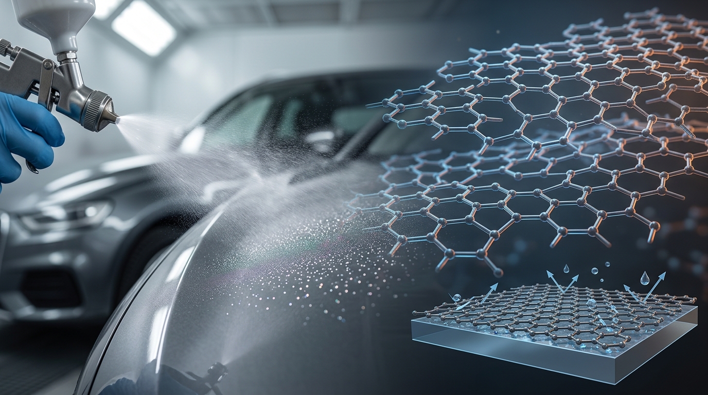
- Membranes and Barrier Films: Pristine graphene networks are completely impermeable to all standard gas molecules, enabling ultra-thin anti-corrosion barriers and molecular-scale water filtration membranes.
Selection Framework: Choosing Between Graphite and Graphene
Engineers selecting between these two materials must evaluate three main criteria: required performance thresholds, processing integration, and unit economics.
When the application requires bulk mass, high volume packing, and low cost—such as filling an electric vehicle battery anode or lining a high-temperature furnace—graphite is the engineered choice. If the application demands extreme surface-to-volume ratios, optical transparency, structural reinforcement at minimal weight, or access to ballistic electron pathways, exfoliated or CVD graphene is the necessary material.