Graphene Sheet
A graphene sheet is a single-atom-thick planar membrane of carbon atoms densely packed into a two-dimensional (2D) honeycomb lattice. Bound together by strong in-plane sp2 covalent bonds, this crystalline structure serves as the fundamental building block for all other graphitic carbon allotropes, including zero-dimensional fullerenes, one-dimensional carbon nanotubes, and three-dimensional stacked graphite.
As an isolated two-dimensional crystal, a pristine graphene sheet exhibits an exceptional combination of mechanical strength, electrical conductivity, thermal transport, optical transparency, and molecular impermeability. In materials science and solid-state physics, understanding how continuous graphene sheets are synthesized, manipulated, and integrated onto functional substrates is central to developing next-generation optoelectronics, thermal management systems, and advanced membrane technologies.
Defining the Graphene Sheet: Structure and Forms
In materials engineering, the term “graphene sheet” typically describes a continuous, macroscopic planar film comprising one to several atomic layers of carbon. However, commercial nomenclature sometimes blurs the distinction between continuous sheets and particulate forms of graphene.
Continuous Large-Area Sheets vs. Graphene Nanoplatelets
It is essential to distinguish continuous 2D films from dispersed graphene powders or flakes:
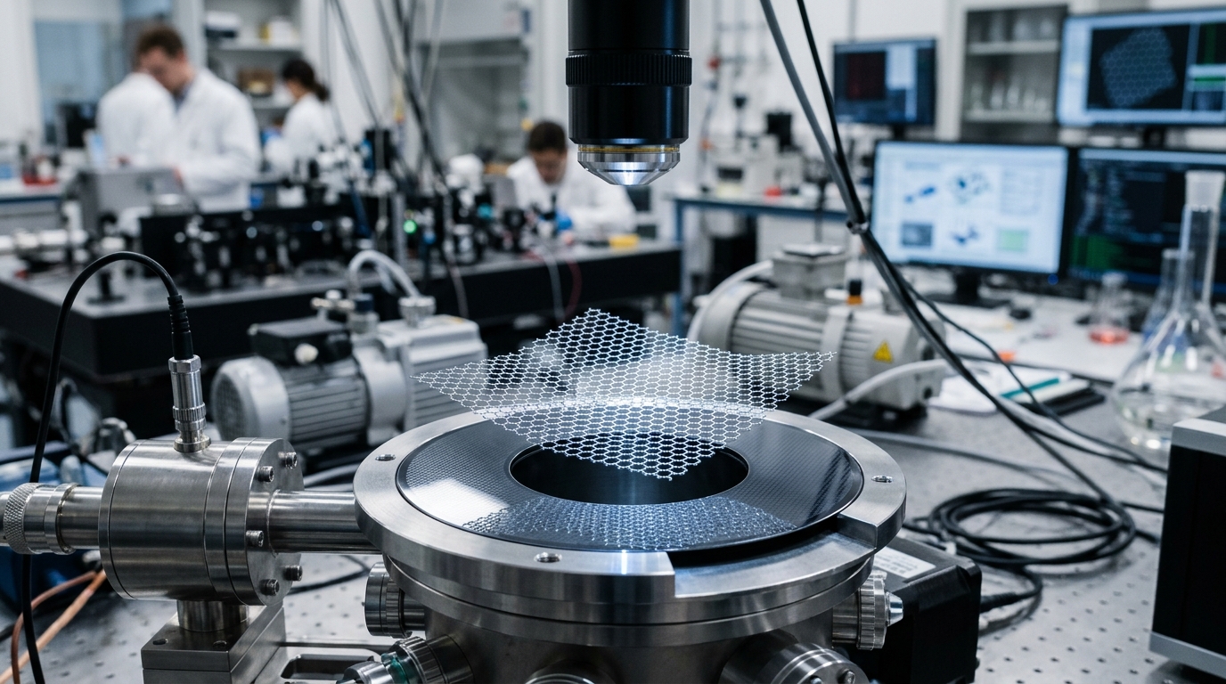
- Continuous Large-Area Graphene Sheets: These are unbroken, wafer-scale or roll-scale 2D films typically synthesized via Chemical Vapor Deposition (CVD) or epitaxial growth. They are characterized by lateral dimensions ranging from millimeters to meters while maintaining a thickness of one to a few atoms. These films are utilized in devices requiring uninterrupted electron pathways, such as touch sensors, transparent conductors, field-effect transistors (FETs), and barrier membranes.
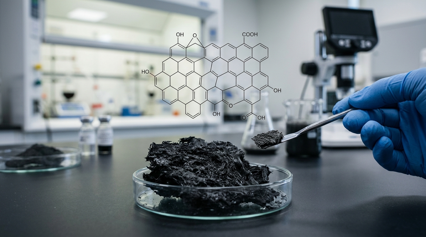
- Graphene Nanoplatelets (GNPs) and Flakes: These consist of microscopic, discontinuous particles with lateral dimensions spanning hundreds of nanometers to several micrometers and thicknesses from 1 to 100 layers. Produced via liquid-phase exfoliation or chemical oxidation-reduction (graphene oxide), flakes are utilized primarily as bulk additives to reinforce polymers, improve battery slurries, or enhance conductive inks.
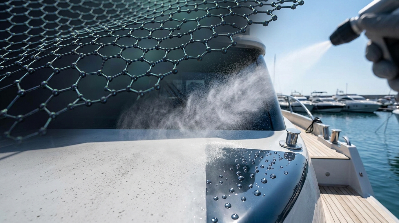
Note on consumer terminology: Commercial bedding products marketed as “graphene sheets” refer to conventional woven textiles (such as polyester, cotton, or rayon) blended with microscopic graphene powder or graphite flakes to promote minor antistatic or heat-dissipation qualities. These consumer textiles are fundamentally distinct from the continuous single-atom-thick 2D sheets used in materials science and electronics.
Structural Classifications: Monolayer, Bilayer, and Few-Layer
The physical and electronic behavior of a graphene sheet depends heavily on the exact number of stacked atomic layers and their crystallographic orientation.
| Classification | Number of Layers | Typical Thickness | Key Electronic and Structural Features |
|---|---|---|---|
| Monolayer Graphene | 1 | ~0.335 nm | Zero-bandgap semimetal, linear Dirac dispersion, maximum intrinsic carrier mobility, ~97.7% optical transmission. |
| Bilayer Graphene | 2 | ~0.67 nm | Parabolic band structure; can be Bernal (AB) stacked or twisted. Electric displacement fields can induce a tunable bandgap up to ~250 meV in AB-stacked sheets. |
| Few-Layer Graphene (FLG) | 3 to 5 | ~1.0 to 1.7 nm | Transition region between 2D behavior and bulk graphite; electronic properties depend on stacking sequence (ABA vs. ABC). |
| Multi-Layer Graphene / Thin Graphite | 6 to 10 | ~2.0 to 3.4 nm | Gradual recovery of bulk graphite electronic properties; diminished optical transparency and decreased charge mobility compared to monolayer. |
Monolayer Graphene
Monolayer graphene is a zero-overlap semimetal. The conduction and valence bands touch at six distinct points known as Dirac points (or K and K’ points in the Brillouin zone). Near these points, charge carriers behave as massless Dirac fermions with a linear energy-momentum dispersion relation. This unique band structure yields extremely high room-temperature electron mobilities because charge carriers experience minimal backward scattering.
Bilayer and Few-Layer Stacking
When a second layer is added, the interaction between the π-orbitals of adjacent sheets modifies the electronic band structure. In Bernal (AB) stacked bilayer graphene, the linear dispersion is replaced by a parabolic dispersion. Applying an external perpendicular electric field breaks the inversion symmetry between the top and bottom sheets, opening a continuous, tunable bandgap—a property absent in pristine monolayer graphene that provides a pathway toward digital switching components.
When layers are rotationally misaligned rather than strictly Bernal-stacked (known as twisted bilayer graphene), moiré superlattices emerge. At specific “magic angles” (approximately 1.1°), the electronic bands flatten significantly, promoting strong electron-electron correlation phenomena such as unconventional superconductivity and correlated insulating states.
Core Intrinsic Properties of a 2D Graphene Sheet
The planar sp2 hybridization of carbon atoms within the graphene sheet—where each carbon atom forms three robust in-plane σ-bonds at 120° angles, with remaining pz orbitals forming a delocalized π-band—endows the material with a rare combination of physical properties.
Mechanical Strength and Elasticity
A defect-free monolayer graphene sheet is one of the strongest materials ever measured. It exhibits an intrinsic ultimate tensile strength of approximately 130 GPa and a Young’s modulus of ~1 TPa (1,000 GPa). Despite its extreme rigidity under in-plane tension, the sheet remains out-of-plane flexible, capable of sustaining elastic strains up to 15–20% without brittle fracture.
Electrical Transport and Carrier Mobility
Due to the absence of bulk scattering centers and the ballistic transport characteristics of Dirac fermions, room-temperature charge carrier mobilities in suspended monolayer graphene can exceed 200,000 cm²/V·s. Even when supported on standard dielectric substrates such as silicon dioxide (SiO2), where substrate roughness and trapped charges induce extrinsic scattering, mobilities frequently range between 10,000 and 40,000 cm²/V·s—far outperforming conventional crystalline silicon.
Thermal Conductivity
Thermal transport in graphene is dominated by acoustic phonons. Freely suspended monolayer graphene displays an in-plane thermal conductivity between 3,000 and 5,000 W/m·K at room temperature, significantly higher than pure copper (~400 W/m·K) and diamond (~2,000 W/m·K). When the sheet is clamped to a substrate, interfacial phonon scattering reduces this value, yet it remains exceptional at roughly 600 to 1,500 W/m·K.
Optical Transparency
A single monolayer of graphene absorbs only a small fraction of incident white light. The optical absorption is determined primarily by the fine-structure constant (α), absorbing approximately 2.3% of light across the visible and near-infrared spectrum. Consequently, a single-layer graphene sheet provides an optical transparency of ~97.7%, with each additional layer adding roughly 2.3% to total optical absorption.
Gas Impermeability
The dense geometric packing of carbon atoms and the overlapping electron cloud of the π-orbitals create a geometric pore size far smaller than standard atomic or molecular radii. As a result, a pristine, defect-free graphene sheet is completely impermeable to all standard gases and liquids under ambient conditions, including helium atoms.
Synthesis and Fabrication Methods
Producing graphene sheets requires balancing material quality, crystal domain size, throughput, and substrate compatibility.
1. Chemical Vapor Deposition (CVD)
Chemical Vapor Deposition is the primary industrial method for producing continuous, large-area graphene sheets.
- Copper Catalyzed CVD: Methane (CH4) and hydrogen gas are introduced into a high-temperature furnace (typically 900–1,050 °C) containing catalytic copper foil. Copper possesses an extremely low carbon solubility. Once the surface is fully covered by a single atomic layer of carbon, the catalytic dehydrogenation of methane terminates automatically, resulting in self-limiting, high-uniformity monolayer graphene.
- Nickel Catalyzed CVD: Nickel has a higher carbon solubility than copper. Carbon dissolves into the bulk metal at high temperatures and precipitates onto the surface during the cooling phase. Because precipitation rates can be difficult to control uniformly across a substrate, nickel CVD often yields multi-layer or inhomogeneous few-layer graphene sheets unless rapid, precise thermal cycles are employed.
2. Mechanical Exfoliation (Micromechanical Cleavage)
Mechanical exfoliation utilizes adhesive tape to overcome the weak van der Waals forces holding together the basal planes of natural or synthetic graphite crystals. Repeated peeling yields isolated monolayer and few-layer graphene sheets deposited onto oxidized silicon wafers. While this method produces flakes with near-zero structural defects—making it the gold standard for fundamental physics research—it cannot scale for commercial manufacturing due to irregular geometries, small domain sizes (typically 10–100 µm), and low throughput.
3. Epitaxial Growth on Silicon Carbide (SiC)
Heating single-crystal silicon carbide wafers to extreme temperatures (>1,300 °C) in an ultra-high vacuum or argon environment causes silicon atoms to sublimate selectively from the surface. The remaining carbon atoms spontaneously rearrange into continuous graphene layers. This method produces high-quality, wafer-scale graphene sheets directly on an insulating or semiconducting substrate, avoiding complex transfer steps. However, high wafer costs and elevated processing temperatures limit its use to specialized electronic applications.
Substrate Transfer Processes
Because CVD graphene is grown on metallic foils, it must usually be transferred onto target substrates—such as silicon wafers, quartz, glass, or flexible polymers—before it can be fabricated into functional devices.
Polymer-Assisted Wet Transfer
The standard laboratory transfer approach involves several sequential steps:
- A sacrificial polymer support layer, typically poly(methyl methacrylate) (PMMA), is spin-coated onto the top surface of the graphene-on-copper stack.
- The underlying copper substrate is chemically etched away using an aqueous etchant solution, such as iron(III) chloride (FeCl3) or ammonium persulfate ((NH4)2S2O8), leaving the PMMA/graphene membrane floating on the liquid surface.
- The floating stack is rinsed in deionized water to remove residual metallic ions and transferred onto the receiving target substrate.
- Once dried and adhered, the PMMA support layer is dissolved using organic solvents such as acetone, leaving the continuous graphene sheet resting on the target surface.
Roll-to-Roll (R2R) Dry Transfer
For scalable industrial production, wet etching is often replaced by continuous roll-to-roll mechanical lamination. Graphene grown on flexible copper foils is laminated against a target film (such as polyethylene terephthalate, or PET) coated with a thermal release tape or UV-curable adhesive. The copper is either electrochemically delaminated (allowing the copper foil to be recycled) or etched, enabling high-speed manufacturing of continuous transparent conductive films.
Primary Technological Applications
Planar graphene sheets are transitioning from fundamental research into commercial integration across several engineering domains.
Transparent Conductive Electrodes
Continuous graphene sheets offer high optical transmittance (~97.7% per layer) combined with low sheet resistance, particularly when chemically doped (e.g., using nitric acid, gold chloride, or conductive polymers). This makes large-area CVD graphene a non-brittle, indium-free alternative to Indium Tin Oxide (ITO) for use in flexible touch screens, organic light-emitting diodes (OLEDs), and organic solar cell electrodes.
Thermal Spreaders and Heat Dissipation
High-power density electronics generate localized hotspots that degrade component performance. Multi-layer graphene sheets and thick stacked graphene films act as lightweight, highly conductive heat spreaders. Because of their in-plane thermal conductivity, these films rapidly disperse heat laterally away from microprocessors, power amplifiers, and compact battery modules.
High-Frequency and RF Electronics
Because pristine graphene lacks an intrinsic bandgap, standard graphene field-effect transistors (GFETs) cannot achieve the high on/off current ratios required for digital logic computing. However, their high carrier mobility and saturation velocity make them well-suited for analog high-frequency and radio-frequency (RF) electronics. GFETs are designed to operate as low-noise amplifiers, frequency multipliers, and ultra-fast optical modulators capable of switching in the gigahertz and terahertz domains.
Molecular Filtration and Separation Membranes
Leveraging its atomic thinness and intrinsic gas impermeability, graphene can be converted into a precision molecular sieve. By introducing sub-nanometer pores into a continuous graphene sheet via controlled plasma etching or ion bombardment, engineers fabricate ultra-thin filtration membranes. These membranes allow selective, high-flux transport of water molecules or specific gases while blocking ions and larger compounds, reducing the energy requirements for water desalination and industrial gas separation.
Biosensors and Chemical Detection
Because every carbon atom in a monolayer graphene sheet is directly exposed to the external environment, surface adsorptions cause measurable shifts in the sheet’s electrical conductivity and Fermi level. Functionalizing the graphene surface with specific receptor molecules enables field-effect biosensors capable of real-time, label-free electrical detection of target proteins, DNA sequences, viral pathogens, and trace gases at picomolar or parts-per-billion concentrations.
Engineering Limitations and Current Challenges
Despite its performance in controlled laboratory settings, integrating continuous graphene sheets into mass manufacturing involves several persistent engineering challenges:
- Grain Boundaries and Point Defects: Polycrystalline CVD graphene sheets consist of individual crystalline domains joined by grain boundaries. These boundaries, along with atomic vacancies and topological defects, act as scattering centers that reduce the theoretical electrical conductivity, thermal transport, and mechanical yield strength of large-scale films.
- Transfer Contamination and Wrinkling: The mechanical handling and chemical transfer of atom-thick membranes can introduce wrinkles, folds, micro-tears, and solvent residue (such as trace PMMA). These physical imperfections degrade device uniformity across large wafer surfaces.
- Direct Growth Limitations: CVD requires temperatures that exceed the thermal budgets of standard processed silicon CMOS wafers (~400–450 °C) and flexible plastic substrates. Developing low-temperature growth chemistries or clean, damage-free dry transfer techniques remains a major research priority.
By refining continuous synthesis protocols, improving dry transfer mechanics, and mitigating crystallographic defects, materials scientists continue to expand the industrial viability of continuous graphene sheets across optoelectronic, thermal, and membrane applications.