Motorola Graphene
When hardware engineers explore methods to push mobile performance beyond physical limits, thermal and structural bottlenecks quickly emerge. In mobile devices, the term motorola graphene refers to the exploration, patenting, and implementation of graphene-based nanomaterials across consumer smartphones, two-way radios, and flexible communications hardware. Rather than replacing silicon microprocessors directly, graphene serves as a functional material to solve heat dissipation, structural durability, flexible transparent conductivity, and radio-frequency transmission challenges.
The Thermal Dilemma in Mobile Device Design
Modern mobile devices operate under strict physical constraints. High-performance system-on-chips (SoCs), fast-charging battery circuits, and dense cellular radio arrays generate concentrated thermal energy. Without active cooling components like motorized fans, smartphones rely on passive thermal dispersion to transfer heat away from the silicon die toward the outer chassis.
Traditional thermal architectures rely on copper foils, vapor chambers, and synthetic graphite sheets. While synthetic graphite provides excellent lateral heat spreading, it exhibits mechanical vulnerabilities when bent repeatedly and possesses lower thermal conductivity than pristine nanocarbon structures. Graphene provides a distinct advantage through its two-dimensional honeycomb lattice of sp2-bonded carbon atoms, which facilitates rapid ballistic phonon transport across its surface.
By integrating multilayer graphene sheets into internal shielding assemblies, hardware designers can move thermal energy away from localized processing hotspots. This prevents thermal throttling, preserves battery longevity, and keeps external touchpoints within safe operating temperatures.
Key Applications of Graphene in Motorola Hardware
Graphene research within mobile communications targets specific material failure points. The primary integration areas span four distinct hardware subsystems:
1. Thermal Management and Heat Spreading
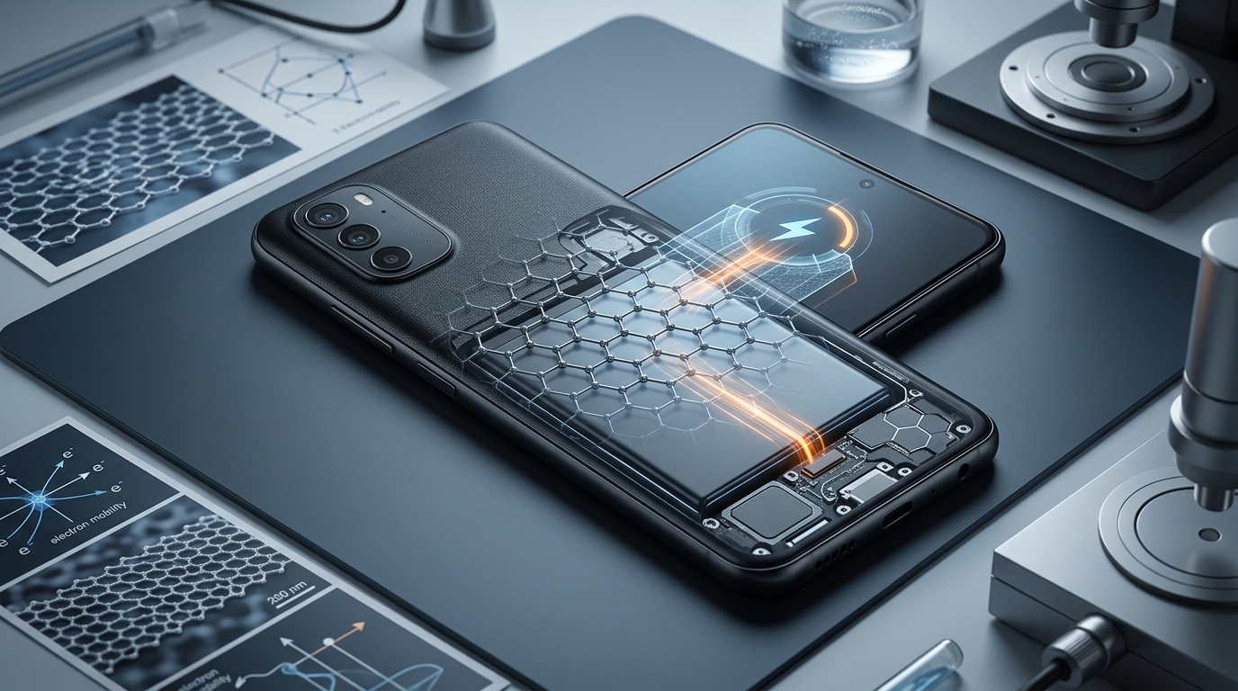
Graphene films applied over battery bays and processing boards act as heat spreaders. Unlike isotropic conductors such as aluminum or copper, engineered graphene films feature highly anisotropic conduction: they dissipate heat across the horizontal surface area at extreme speeds while moderating heat flow vertically. This directional dissipation prevents heat from migrating into the display panel or battery cells.
2. Flexible and Foldable Electronics
The transition toward clamshell and book-style foldable smartphones introduces severe mechanical demands along the hinge axis. Traditional transparent electrodes rely on indium tin oxide (ITO), a ceramic material that micro-fractures after repeated folding cycles. Graphene films serve as flexible transparent conductors capable of withstanding hundreds of thousands of bending cycles without sacrificing electrical continuity or optical transparency.
3. Radio Frequency (RF) and Antenna Components
High-frequency communication bands require compact antenna structures that minimize resistive energy losses. Graphene-enhanced conductive inks and composite coatings allow engineers to print low-profile antenna arrays directly onto interior chassis walls or flexible printed circuits. These materials provide corrosion resistance, reduce component weight, and maintain stable electromagnetic performance across broad frequency ranges.
4. Battery Electrodes and Conductive Additives
In power systems, graphene functions primarily as a conductive additive rather than a standalone anode. Introducing graphene platelets into standard lithium-ion cathode and anode slurries builds a percolating electrical network. This network lowers the internal cell resistance, allowing faster discharge and recharge cycles while controlling internal heat generation.
Material Forms: CVD Films vs. Exfoliated Platelets
In hardware manufacturing, the performance of graphene depends entirely on how the material is synthesized and integrated. The industry distinguishes between two primary production methods, each suited to different device components:
- Chemical Vapor Deposition (CVD) Graphene: Grown on catalytic metal substrates, CVD produces continuous single-layer or few-layer films. This technique yields exceptional optical transparency and carrier mobility, making it the primary candidate for touch sensors, optical layers, and flexible display electrodes. However, high fabrication costs and transfer complexity limit broad deployment.
- Liquid-Phase Exfoliation (LPE) and Nanoplatelets: Produced by shearing raw graphite flakes in liquid solutions, this method yields bulk powders and suspensions containing liquid-phase exfoliation byproducts. These platelets are blended into polymers, pastes, and thermal interface materials (TIMs). While lacking the pristine crystal structure of CVD sheets, exfoliated platelets provide cost-effective electrical and thermal percolation networks suitable for mass-market manufacturing.
Thermal Dissipation Material Comparison
To understand why hardware developers integrate nanocarbon films, consider how graphene compares to conventional thermal conductors in mobile applications:
| Material Form | In-Plane Thermal Conductivity (W/m·K) | Mechanical Flexibility | Primary Mobile Function |
|---|---|---|---|
| Standard Copper Foil | 380 – 400 | Moderate (Prone to work hardening) | Vapor chamber shells, ground planes |
| Pyrolytic Synthetic Graphite | 700 – 1,500 | Low to Moderate (Delaminates under sharp creasing) | Standard chassis heat spreaders |
| Multilayer Graphene Film | 1,200 – 2,000+ | High (Maintains structure under repeated flex) | High-efficiency heat spreaders, foldable hinges |
| Graphene-Infused Thermal Paste | 5 – 15 | Not Applicable (Viscous fluid/gel) | SoC-to-shielding junction interfaces |
Technical Challenges and Engineering Tradeoffs
Despite its theoretical performance, integrating graphene into mass-produced communications hardware presents notable engineering trade-offs:
Interfacial Thermal Resistance
A material with extreme in-plane thermal conductivity can still underperform if heat cannot efficiently enter and exit the film. The boundary between silicon packaging, adhesive layers, and the carbon film creates interfacial thermal resistance (also known as Kapitza resistance). If the adhesive used to secure a graphene sheet acts as a thermal insulator, the material advantages are substantially degraded.
Substrate Transfer and Defects
Single-layer films grown via chemical vapor deposition must be separated from their growth substrates and transferred onto target electronics without creating wrinkles, cracks, or metallic contamination. Even minor lattice defects scatter phonons and electrons, causing real-world performance to fall short of theoretical calculations.
Cost-to-Benefit Ratio
Synthetic graphite remains an established, low-cost thermal solution. Replacing synthetic graphite with advanced graphene films increases bill-of-materials costs. Hardware manufacturers must therefore evaluate whether the marginal drop in operating temperature justifies the higher processing and material expenses for a given product tier.
Common Misconceptions
Discussions surrounding graphene in mobile technology often blend laboratory experiments with mass production realities. Addressing these distinctions clarifies how the material actually functions:
- Misconception: Mobile processors are made entirely of graphene. Silicon remains the foundational semiconductor for microprocessors. Graphene lacks a natural electronic bandgap, meaning it cannot easily switch off to represent binary states without complex chemical modifications that degrade its mobility.
- Misconception: A graphene battery charges in seconds. Graphene in commercial batteries acts as a thermal and conductive additive inside the electrode matrix. It does not replace the fundamental lithium-ion chemistry; instead, it reduces internal impedance to enable safer high-current charging.
- Misconception: Any black film inside a phone is pure graphene. Many commercial heat spreaders labeled as graphene are composite materials containing compressed graphite powders mixed with polymer binders and minor graphene fractions.
Evaluating Graphene Integration in Modern Devices
When assessing how graphene enhances mobile technology, hardware analysts examine specific performance metrics rather than promotional claims. The effectiveness of nanocarbon integration is verified through several criteria:
- Sustained Clock Speeds: Measuring how long an onboard processor maintains peak frequency during prolonged computation without thermal throttling.
- Surface Temperature Delta: Calculating the temperature gradient between the internal processor die and the external chassis surface to confirm efficient heat dissipation.
- Flexural Fatigue Life: Testing flexible printed interconnects and display electrodes across thousands of dynamic bend cycles to verify structural integrity along mechanical hinges.
- Component Mass Reductions: Replacing heavier metallic shielding plates with ultra-thin carbon films to reduce overall device weight while maintaining electrical ground integrity.
The application of graphene within mobile hardware demonstrates how advanced materials science resolves physical constraints in compact electronics. By deploying graphene where standard metals and plastics fall short—specifically in directional thermal management and resilient flexible circuits—hardware engineers continue to refine the efficiency, durability, and form factors of modern communications hardware.