Graphene Cost
The commercial graphene cost varies dramatically depending on material grade, crystal quality, layer count, and physical form factor. Graphene is not a singular commodity traded at a single benchmark price; instead, the market spans several orders of magnitude. Industrial-grade bulk powders such as graphene nanoplatelets (GNPs) sell for $20 to $100 per kilogram in multi-tonne volumes, while continuous chemical vapor deposition (CVD) single-layer films for electronics are priced by surface area at $0.05 to $2.00 per square centimeter at industrial scale, or up to $25 to $100 per square centimeter for specialized research substrates.
Understanding real-world graphene pricing requires distinguishing between high-volume bulk additives (used in composites, concrete, and energy storage) and high-purity crystalline sheets (used in photonics, semiconductors, and precision sensors).
Graphene Cost Breakdown by Material Grade and Form Factor
Commercial graphene products fall into two primary manufacturing categories: top-down exfoliation of graphite (yielding powders, flakes, and dispersions) and bottom-up synthesis from hydrocarbon precursors (yielding thin films and wafer-scale materials). Each synthesis method produces distinct properties, yield profiles, and cost structures.
| Material Grade / Form Factor | Primary Synthesis Route | Unit Metric | Lab / Research Price (< 100 g / single wafer) | Industrial Bulk Price (Tonne / Contract Volume) |
|---|---|---|---|---|
| Graphene Nanoplatelets (GNP) | Liquid-phase / shear exfoliation, plasma | Per gram / Per kg | $10 – $50 / g ($10,000 – $50,000 / kg) | $20 – $100 / kg ($0.02 – $0.10 / g) |
| Graphene Oxide (GO) | Modified Hummers’ chemical oxidation | Per gram / Per kg | $50 – $200 / g | $50 – $200 / kg ($0.05 – $0.20 / g) |
| Reduced Graphene Oxide (rGO) | Thermal, chemical, or electrochemical reduction | Per gram / Per kg | $100 – $300 / g | $100 – $500 / kg |
| CVD Monolayer / Few-Layer Films (on Cu) | High-temperature CVD growth | Per cm² | $25 – $100 / cm² | $0.05 – $2.00 / cm² (Roll-to-roll / large-area) |
| Transferred CVD Films (SiO₂/Si, Quartz, PET) | CVD growth + post-growth film transfer | Per wafer / Per unit | $150 – $800 / unit (2″ to 4″ wafer) | Custom B2B contract pricing |
Graphene Nanoplatelets (GNP)
Graphene nanoplatelets consist of stacks of multi-layer graphene ranging from 2 to several dozen carbon layers. Produced via mechanical shearing, liquid-phase exfoliation, or plasma cracking of natural graphite, GNPs represent the highest-volume segment of the market. At industrial purchasing tiers, bulk GNPs reach the $20 to $100 per kg floor, making them economically viable as mechanical reinforcement agents, barrier coatings, and thermal or conductive additives in polymers and battery electrodes.
Graphene Oxide (GO) and Reduced Graphene Oxide (rGO)
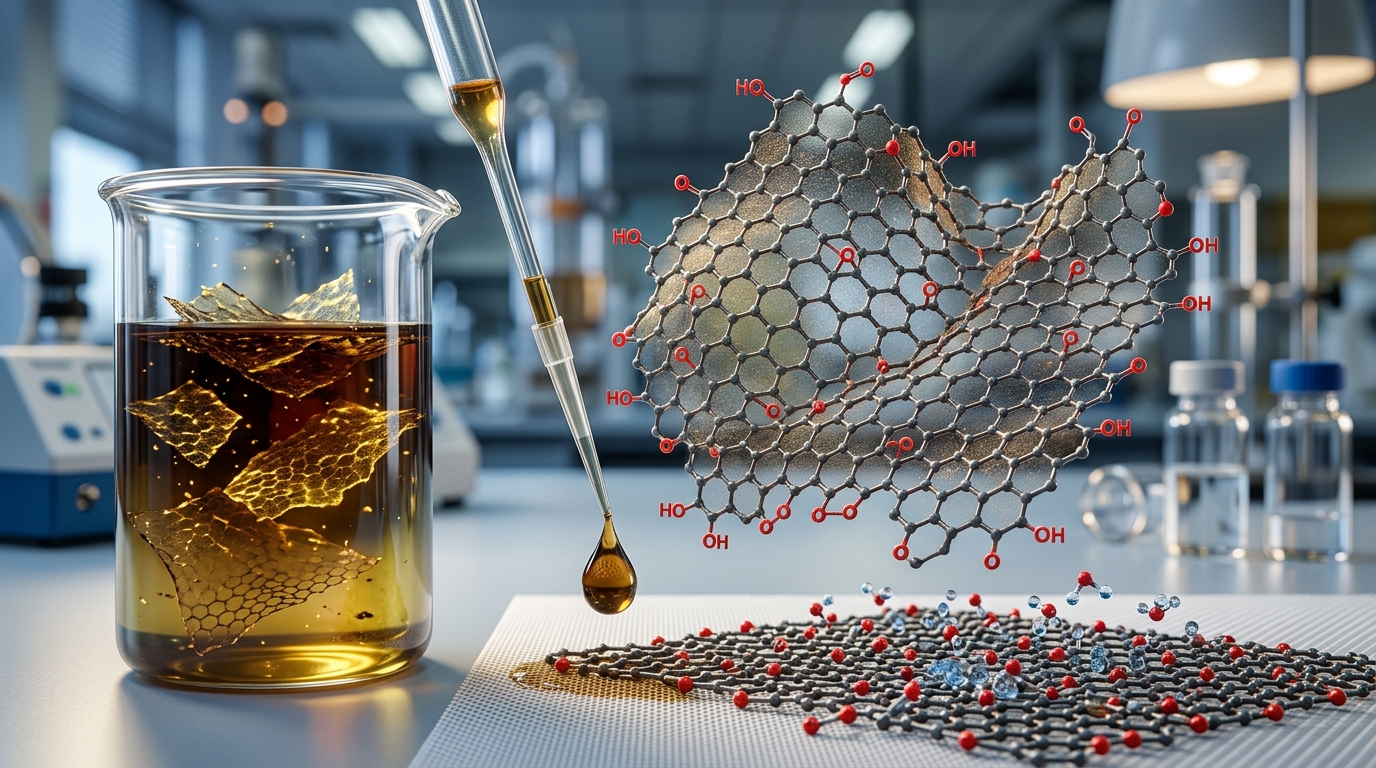
Graphene oxide is synthesized by exposing flake graphite to aggressive oxidizers (typically potassium permanganate and concentrated sulfuric acid via the modified Hummers’ method). The resulting oxygen-functionalized carbon sheets are hydrophilic and readily disperse in water. Pure GO powder sells for $50 to $200 per kg in bulk. When interpreting GO pricing, buyers must verify whether quotes refer to dry carbon content or total solution weight, as GO is frequently supplied as a 0.5 to 4.0 mg/mL aqueous dispersion.
Reduced graphene oxide (rGO) partially restores electrical conductivity by removing oxygen-containing functional groups through thermal annealing or chemical reducing agents. Because reduction adds an additional processing step and chemical overhead, rGO commands higher prices, ranging from $100 to $500 per kg at commercial volumes.
CVD Single-Layer and Few-Layer Films
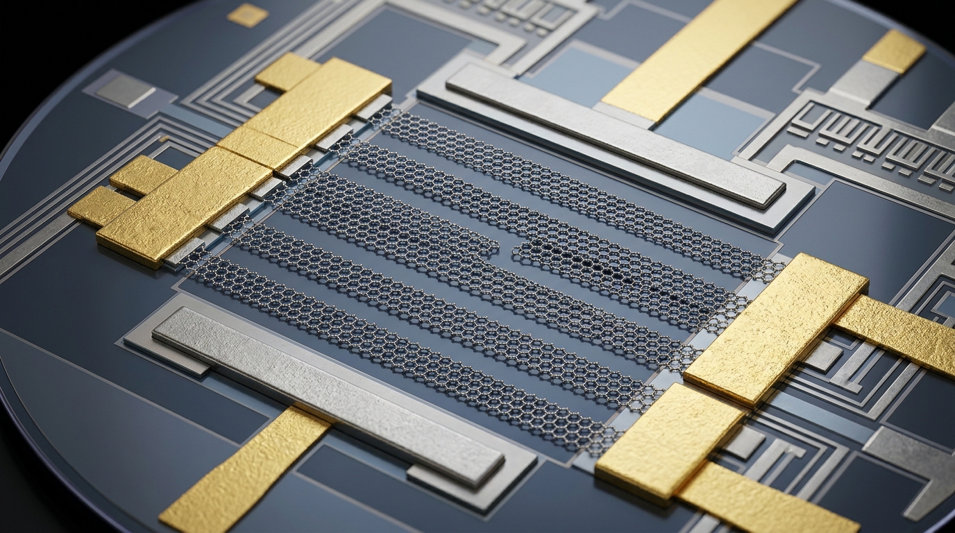
High-temperature chemical vapor deposition deposits carbon atoms from gaseous precursors (such as methane) onto catalytic metal substrates (typically copper or nickel foil). CVD graphene offers superior crystalline perfection, exceptional carrier mobility, and optical transparency, but it cannot be evaluated on a mass basis.
Because theoretical single-layer graphene weighs only approximately 0.77 milligrams per square meter, pricing CVD films by mass yields theoretical figures between $10,000 and $290,000+ per kilogram. Consequently, CVD films are sold strictly by area or unit wafer size. As-grown films on copper foils range from $0.05 to $2.00 per cm² in large industrial batches, while films cleanly transferred to target dielectric substrates (such as silicon wafers with thermal oxide layers) carry substantial post-processing premiums.
Lab-Scale vs. Commercial Bulk Purchasing Dynamics
The gap between laboratory catalog pricing and industrial master supply agreements is wider for graphene than for conventional specialty chemicals. This spread is driven by packaging, handling, distributor markups, and characterization guarantees.
- Research Quantities (< 100 g or Single Wafers): Sourced through standard chemical distributors and catalog suppliers, small-quantity orders carry high unit costs ($10 to $50 per gram for GNPs; $150 to $800 per transferred wafer). These prices reflect specialized packaging (inert atmosphere sealing, cleanroom containers), individual batch certification, and low-volume processing costs.
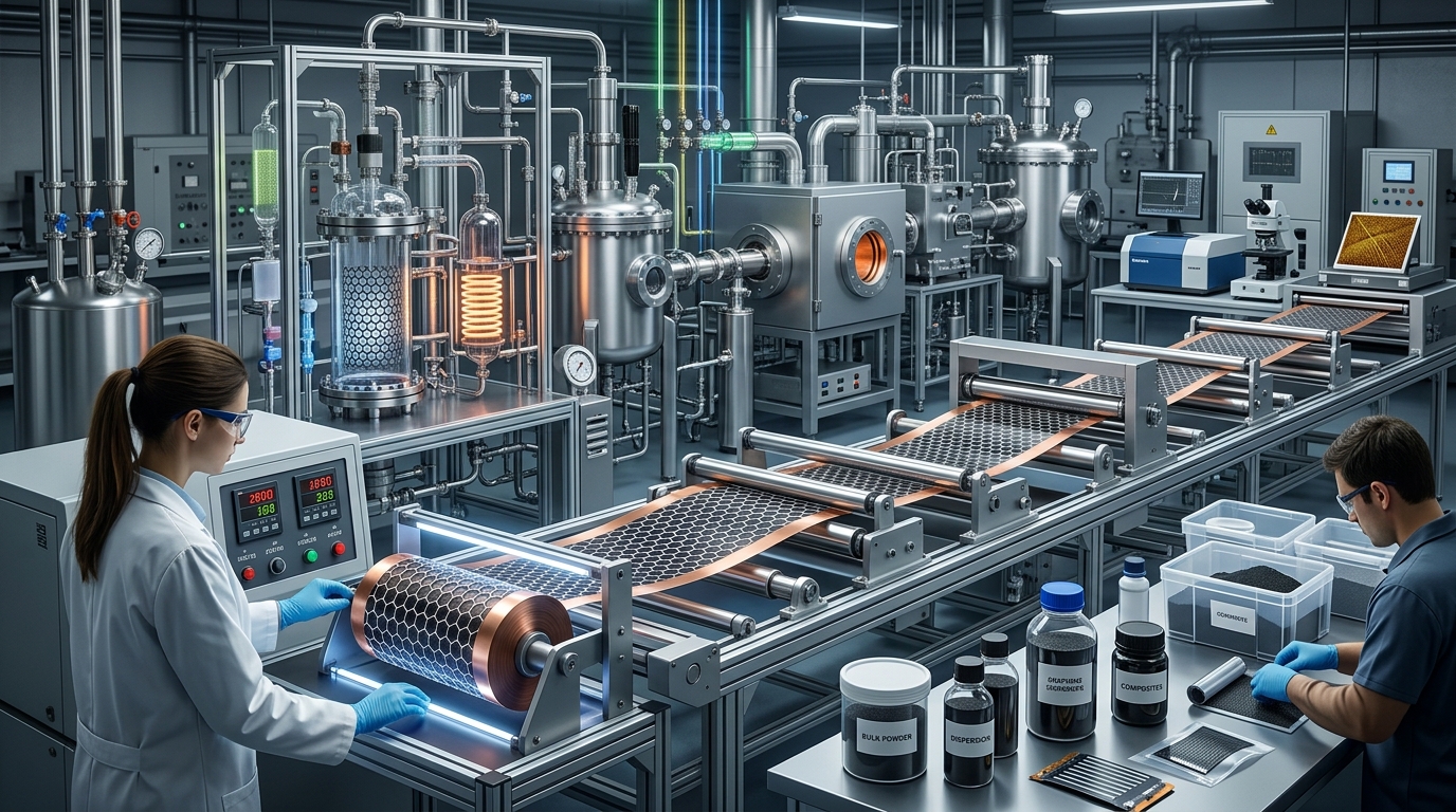
- Industrial Bulk (> 1 Tonne or Roll-to-Roll Contracts): High-volume commercial procurement bypasses intermediate distributors through direct, long-term supply agreements. Bulk economies of scale reduce GNP pricing down to $20 to $50 per kg, positioning graphene to compete directly with high-performance carbon black, carbon nanotubes (CNTs), and fine synthetic graphite in battery anodes, structural composites, and industrial coatings.
Major Drivers of Graphene Manufacturing Costs
The total cost to manufacture graphene is dictated by four primary variables: synthesis energy, substrate handling, raw feedstock purity, and analytical quality control.
1. Synthesis Method and Energy Intensity
Every production route involves distinct thermodynamic and operational constraints:
- CVD Processes: Require high operating temperatures (900 °C to 1,100 °C), controlled vacuum or inert gas atmospheres, and specialized quartz tube or cold-wall reactors, resulting in high electrical and capital equipment expenses.
- Chemical Oxidation (GO/rGO): While operating at lower temperatures, wet chemical oxidation produces substantial acid waste. Neutralizing, washing, and treating hazardous effluent (sulfuric acid and manganese salts) represents a major component of operational expenditure (OPEX).
- Mechanical/Liquid Exfoliation: Mechanically shearing graphite exhibits lower chemical inputs but requires prolonged processing cycles and high-shear energy to achieve uniform exfoliation without excessive structural damage.
2. Substrate and Transfer Bottlenecks (CVD)
For CVD graphene intended for semiconductor or optoelectronic applications, the catalytic copper foil substrate is only the first cost component. The subsequent transfer process represents the single largest yield and cost bottleneck. Delaminating the atomic monolayer from copper and transferring it onto target substrates (such as silicon, quartz, or flexible PET) using sacrificial polymer layers (like PMMA) frequently introduces mechanical tears, wrinkles, and metallic contamination. Low transfer yields directly elevate finished wafer costs.
3. Feedstock Quality
Top-down exfoliation relies on natural or synthetic flake graphite. Achieving high yields of few-layer sheets requires high-purity natural flake graphite (exceeding 99% carbon purity). Fluctuations in mined graphite supply and purification processing directly impact upstream production costs.
4. Metrology and Quality Verification
Rigorous structural verification creates a substantial pricing divide between characterized and uncharacterized carbon materials. Certified grades command a 2× to 5× pricing premium because reliable verification requires advanced analytical instrumentation:
- Raman Spectroscopy: Measures defect densities through the $I_D/I_G$ peak ratio and identifies layer thickness via the 2D band.
- Atomic Force Microscopy (AFM): Quantifies exact vertical step heights and sheet thickness down to the sub-nanometer scale.
- Transmission Electron Microscopy (TEM): Verifies crystal domain alignment and edge structures.
- X-ray Photoelectron Spectroscopy (XPS): Determines exact carbon-to-oxygen ratios and functional group distributions.
Market Risks: The “Fake Graphene” Challenge
A critical issue impacting market pricing is the prevalence of sub-standard carbon powders marketed as pristine graphene at unusually low prices. Under the international standard ISO/TS 80004-13, materials consisting of more than 10 stacked carbon layers are classified as thin graphite or exfoliated graphite rather than graphene.
Many low-cost suppliers sell inexpensive, minimally exfoliated graphite powders (often containing 20 to 100+ layers) under graphene branding. While these materials are cheap to produce, they lack the specific surface area, electrical conductivity, and mechanical reinforcement properties of genuine few-layer graphene (1 to 5 layers) or single-layer sheets, leading to failed formulation trials in industrial settings.
Historical Price Trajectory and Industrial Outlook
Since its initial mechanical isolation, graphene pricing has undergone substantial deflation. In 2010, research-grade flakes routinely commanded tens of thousands of dollars per gram, and commercial-scale quantities were virtually non-existent. Between 2015 and 2026, the construction of multi-ton production facilities across North America, Europe, and Asia expanded global supply, driving bulk powder costs down by more than 80% to 90%.
As prices stabilize near commodity thresholds, adoption is expanding into cost-sensitive, high-volume industries:
- Infrastructure and Concrete: GNPs incorporated at low loading fractions (0.01% to 0.05% by weight) enhance compressive strength and accelerate curing, where material costs must remain below strict per-ton additive budgets.
- Energy Storage: Graphene conductive additives in lithium-ion battery cathodes and silicon-composite anodes provide lower internal resistance and faster charging, competing directly with established carbon black grades.
- Automotive and Aerospace Composites: Thermoplastic and thermoset polymer masterbatches use functionalized graphene to reduce vehicle component weight while preserving mechanical stiffness.
For high-end electronics and photonics, the final cost barrier remains the maturation of continuous roll-to-roll direct growth and high-yield, polymer-free transfer techniques that can deliver high-performance monolayers directly onto functional substrates at line speeds.