Graphene Films
Graphene films represent the continuous, large-area macroscopic form of single- or few-layer carbon atoms arranged in a two-dimensional honeycomb lattice. Unlike graphene powders, nanoplatelets, or liquid dispersions designed as additives for bulk matrices, a graphene film is engineered as an unbroken sheet. This structural continuity allows it to preserve the intrinsic electrical conductivity, thermal transport, optical transparency, and mechanical robustness of the carbon lattice across macroscopic dimensions.
The utility of graphene films spans multiple engineering disciplines. In optoelectronics, they function as ultra-thin, flexible electrodes. In consumer electronics and power systems, thick assembled films serve as directional heat dissipation layers. In chemical engineering, their dense atomic packing provides an impermeable barrier against gases and corrosive elements. Realizing these benefits in practical hardware requires a balance between synthesis methods, film transfer integrity, and the physical trade-offs imposed by microscopic defects.
Film Morphology: Monolayer, Multilayer, and Assembled Sheets
The term graphene film encompasses several distinct structural formats, each characterized by its layer count, crystallographic alignment, and macroscopic continuity.
- Monolayer Films: A single carbon layer with a thickness of roughly 0.335 nanometers. A pristine monolayer absorbs approximately 2.3% of incident white light, offering an exceptional optical transmittance of 97.7%. Monolayers feature the highest theoretical electron mobility, making them ideal for high-speed field-effect transistors, photodetectors, and ultra-sensitive biological sensors.
- Few-Layer Films (2 to 10 Layers): Stacking several graphene sheets reduces sheet resistance and boosts chemical stability, though it reduces optical transparency by approximately 2.3% per additional layer. Bilayer and trilayer films are frequently selected for transparent conductors where lower electrical resistance is prioritized over absolute optical clarity.
- Macroscopic Assembled Films (Graphitic Foils and Papers): Ranging from hundreds of nanometers to tens of micrometers in thickness, these films are fabricated by aligning and consolidating chemical graphene flakes or reduced graphene oxide. While opaque, they deliver immense in-plane thermal conductivity and mechanical flexibility, functioning as lightweight thermal management sheets.
Synthesis Techniques for Large-Area Graphene Films
Producing continuous films requires synthesis platforms capable of maintaining atomic uniformity over meters of surface area. Several primary manufacturing pathways dominate modern production.
Chemical Vapor Deposition (CVD)
Chemical vapor deposition on catalytic metal substrates is the premier route for high-quality, large-area monolayer and few-layer films. In a standard CVD furnace, a hydrocarbon precursor gas (such as methane) is introduced at elevated temperatures, typically between 900 and 1050 degrees Celsius, over a transition metal substrate.
Copper foil is the most common substrate for monolayer growth because of its low carbon solubility. The growth mechanism on copper is self-limiting: methane catalytically decomposes on the exposed copper surface until a single layer of graphene covers the metal, terminating the reaction. Nickel, by contrast, exhibits high carbon solubility at elevated temperatures. Carbon dissolves into the nickel matrix during heating and precipitates to the surface during cooling, yielding multilayer films whose thickness is controlled by cooling rates.
Epitaxial Growth on Silicon Carbide (SiC)
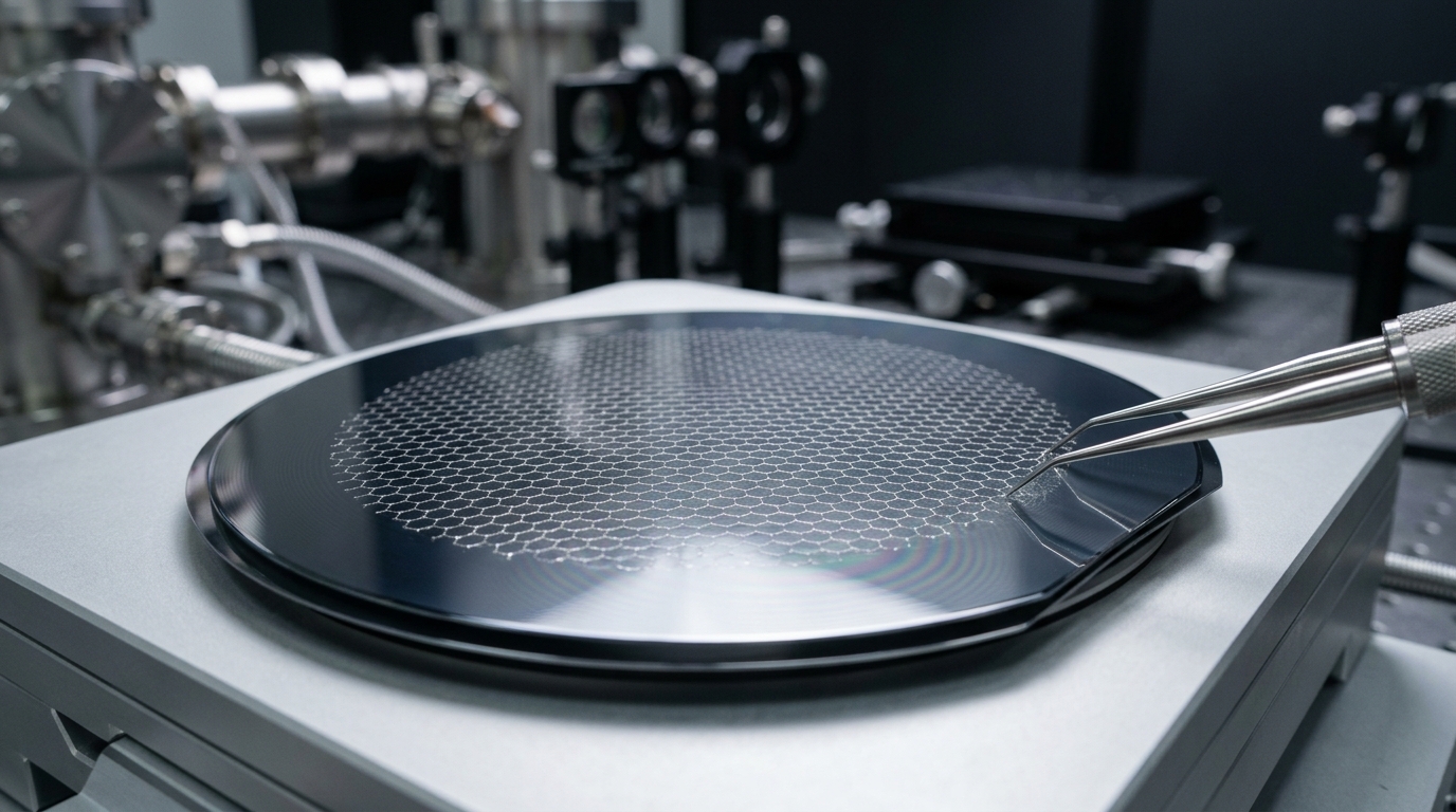
Epitaxial sublimation involves heating single-crystal silicon carbide wafers to temperatures above 1300 degrees Celsius under ultra-high vacuum or an argon environment. Silicon atoms selectively sublime from the surface, leaving behind residual carbon atoms that spontaneously reorganize into epitaxial graphene layers. This process produces high-quality wafer-scale films directly on an insulating or semi-insulating substrate, bypassing the mechanical transfer steps required by metal-catalyzed CVD.
Liquid-Phase Assembly and Reduction
For applications where atomic perfection is secondary to cost and scale, films are assembled from liquid suspensions of graphene oxide (GO). Aqueous GO solutions are cast onto substrates using slot-die coating, spray deposition, or vacuum filtration. The resulting membranes are chemically or thermally treated to remove oxygen functional groups, producing reduced graphene oxide (rGO) films. These assembled sheets exhibit lower carrier mobility than CVD films due to residual structural defects, but they excel in thermal spreading and electromagnetic interference shielding.
The Substrate Transfer Process
Because CVD graphene forms on metal catalysts, integrating the film into functional electronic or optical devices requires detaching it from the growth foil and transferring it onto target substrates, such as glass, silicon dioxide, or flexible polymers.
Wet Chemical Transfer
In conventional wet transfer, a sacrificial polymer support—typically polymethyl methacrylate (PMMA)—is spin-coated onto the top surface of the graphene. The underlying metal foil is chemically dissolved in an etchant bath, such as iron chloride or ammonium persulfate. The floating PMMA/graphene stack is rinsed in deionized water, scooped onto the target substrate, and dried. Finally, the polymeric transfer layer is dissolved using an organic solvent such as acetone.
Roll-to-Roll and Dry Delamination
Wet transfer introduces polymer residue, wrinkles, and micro-cracks that degrade film performance. To enable industrial scale, roll-to-roll processing utilizes thermal release tapes or pressure-sensitive adhesives to mechanically peel the graphene layer from the metal foil. Electrochemical delamination (bubbling transfer) offers another clean alternative: by applying a small voltage to the metal growth substrate in an electrolyte bath, hydrogen gas bubbles form at the interface between the metal and graphene, gently lifting the film without consuming the underlying foil.
Performance Characteristics and Engineering Trade-Offs
Designing devices with graphene films requires balancing competing material properties dictated by synthesis quality, layer count, and post-transfer processing.
| Film Property | Ideal Monolayer Value | Practical CVD Film (Polycrystalline) | Assembled rGO Thick Film |
|---|---|---|---|
| Optical Transmittance (550 nm) | 97.7% | 95% – 97% | Opaque (< 10%) |
| Sheet Resistance | ~30 Ω/sq (doped) | 200 – 1,000 Ω/sq | 10 – 100 Ω/sq |
| Carrier Mobility (Room Temp) | > 200,000 cm²/V·s (suspended) | 1,000 – 5,000 cm²/V·s | 1 – 100 cm²/V·s |
| In-Plane Thermal Conductivity | ~5,000 W/m·K | 1,500 – 3,000 W/m·K | 800 – 1,600 W/m·K |
| Dominant Failure Mode | Intrinsic lattice rupture | Grain boundary tearing | Inter-flake sliding |
Optoelectronic Trade-Off: Transmittance vs. Sheet Resistance
In transparent electrode applications, low sheet resistance and high optical transmittance are simultaneously required. While a single layer of pristine graphene boasts high transparency, its intrinsic sheet resistance is often too high for direct use in displays or photovoltaics. Increasing the layer count lowers sheet resistance but reduces transparency. To circumvent this limitation, chemical dopants such as nitric acid, gold chloride, or conductive polymers are applied to introduce charge carriers without significantly impeding optical transmission.
Structural Imperfections: Grain Boundaries and Wrinkles
Large-area CVD films are inherently polycrystalline, composed of individual crystalline grains stitched together. The junctions between these grains, known as grain boundaries, introduce atomic scattering centers that lower electrical conductivity and mechanical tensile strength. Furthermore, thermal expansion mismatch between the metal growth foil and the carbon lattice causes out-of-plane wrinkles during cooling, creating topographic variations that influence contact resistance in semiconductor junctions.
Practical Applications of Graphene Films
Graphene films have transitioned from basic research into distinct commercial and industrial roles based on their physical formats.
Transparent Conductive Electrodes for Flexible Electronics
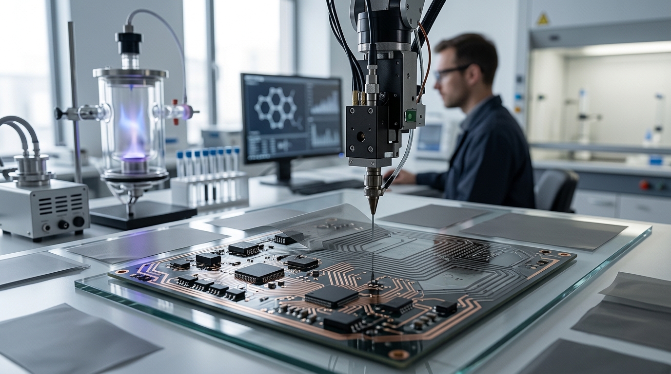
Indium tin oxide (ITO) has historically dominated transparent electrodes, but its brittle nature makes it unsuitable for flexible, foldable displays and wearable electronics. CVD graphene films withstand repetitive bending cycles without significant loss of electrical continuity. When integrated with flexible plastic substrates, graphene electrodes serve as the active conductive matrix in capacitive touch panels, flexible organic light-emitting diode (OLED) displays, and thin-film solar cells.
Thermal Spreading and Heat Dissipation
High-density microelectronics, 5G communication modules, and fast-charging battery packs generate localized hot spots that degrade system reliability. Thick assembled graphene films serve as lightweight thermal spreaders. Their exceptionally high in-plane thermal conductivity rapidly pulls heat away from concentrated processing units and diffuses it laterally across the chassis, outperforming standard copper and aluminum heat spreaders at a fraction of the weight.
Gas and Moisture Barrier Layers
Due to the dense electron cloud of the aromatic carbon ring, a defect-free graphene lattice is impermeable to standard gases, including helium and water vapor. Single- and multi-layer films act as ultra-thin protective coatings against atmospheric oxidation and chemical corrosion. In packaging sensitive organic electronics, graphene barrier films protect organic layers from ambient moisture ingress, extending operating lifetimes without adding bulk.
Biochemical Sensors and Analytical Membranes
Because every carbon atom in a monolayer film is directly exposed to the surrounding environment, even minor chemical or biological adsorption events alter the film’s electrical resistance. Graphene field-effect transistor (GFET) biosensor films detect specific proteins, viral particles, DNA sequences, and heavy metal ions at picomolar concentrations. The film’s surface can be functionalized with specific antibodies or aptamers to bind target analytes selectively.
Characterization and Quality Metrics
Verifying the quality of a graphene film is essential for process control and device integration. Laboratories and fabrication facilities rely on standardized analytical tools to assess structural integrity:
- Raman Spectroscopy: The primary non-destructive characterization tool. The intensity ratio and peak shape of the G band (around 1580 cm⁻¹) and the 2D band (around 2700 cm⁻¹) identify layer count and stacking order. The presence and intensity of the D band (around 1350 cm⁻¹) provide a direct quantitative assessment of atomic lattice defects and grain boundaries.
- Four-Point Probe Resistivity Testing: Measures macroscopic sheet resistance while eliminating contact resistance artifacts, ensuring the film meets electrical conductivity specifications across large surface areas.
- Atomic Force Microscopy (AFM): Evaluates nanoscale surface topography, verifying film thickness, cross-sectional uniformity, wrinkle density, and the presence of residual polymer contamination after transfer.
- UV-Vis Spectrophotometry: Measures optical transmittance across ultraviolet, visible, and infrared spectra to calculate the optoelectronic figure of merit when compared against sheet resistance.
Engineering Selection: CVD vs. Solution-Assembled Films
Specifying a graphene film depends entirely on the primary performance requirements of the end product:
For microelectronics, high-frequency transistors, sensitive optical detection, and flexible transparent touchscreens, monolayer to few-layer CVD films are mandatory. These applications demand high carrier mobility, uniform work functions, and high optical transmittance, where the higher cost of catalytic growth and precision transfer is technically justified.
For thermal management sheets, electromagnetic interference (EMI) gaskets, structural anti-corrosion barriers, and large-scale battery current collectors, thick solution-assembled rGO films offer the optimal solution. These applications benefit from simplified roll-to-roll liquid deposition, self-supporting mechanical thickness, and cost structures aligned with industrial manufacturing scales.