Graphene Material
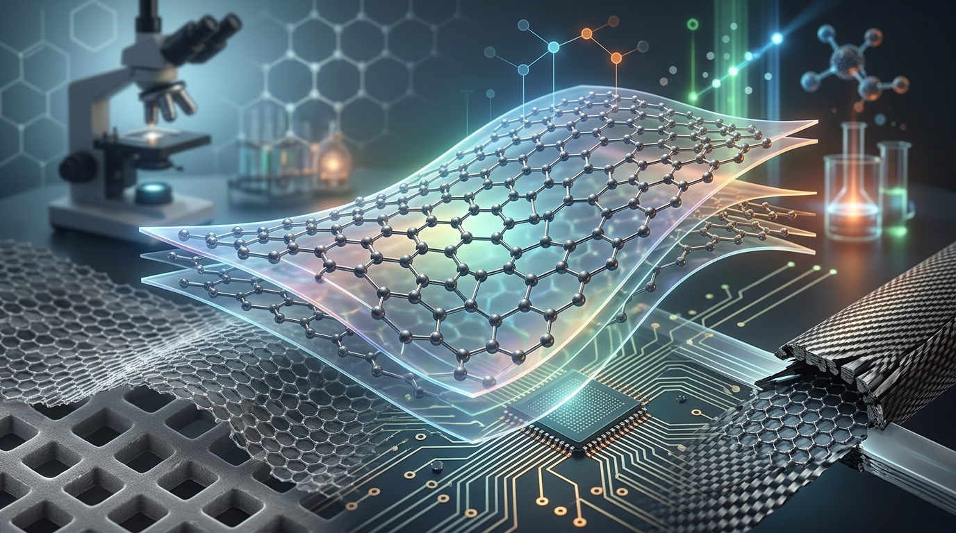
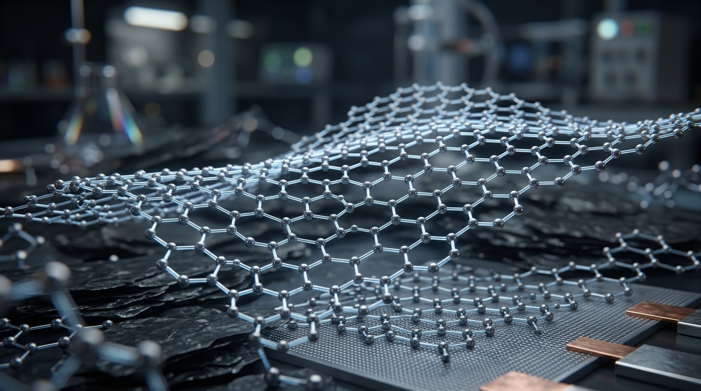
Graphene material is a two-dimensional allotrope of carbon consisting of a single layer of carbon atoms arranged in a hexagonal, honeycomb lattice. Since its isolation and characterization in 2004—an achievement recognized with the 2010 Nobel Prize in Physics—graphene has transitioned from an academic curiosity to one of the most rigorously researched nanomaterials in modern engineering. Because each carbon atom forms strong covalent sp2 bonds with three neighboring atoms, graphene exhibits an extraordinary combination of mechanical strength, electrical conductivity, thermal dissipation, and optical transparency.
Understanding the science, classifications, synthesis routes, and functional limitations of graphene is essential for evaluating its commercial role across aerospace, electronics, energy systems, and advanced manufacturing.
Fundamental Properties of Graphene Material
The macroscopic behaviors observed in graphene materials stem directly from its planar atomic architecture and the quantum mechanical behavior of its delocalized electrons. While individual graphene sheets possess theoretical upper limits of performance, engineered forms exhibit distinct property profiles depending on layer count, defect density, and chemical functionalization.
Mechanical Strength and Elasticity
Graphene is recognized as one of the strongest materials ever measured. Pristine monolayer graphene exhibits an intrinsic tensile strength of approximately 130 GPa and an elastic modulus (Young's modulus) of roughly 1 TPa (1,000 GPa). These values reflect the high energy required to break the planar carbon-carbon covalent bonds. Despite its extreme stiffness, graphene is remarkably flexible and can be reversibly stretched by up to 20% of its initial length without permanent plastic deformation.
Electrical Conductivity and Charge Transport
In pristine graphene, carbon's fourth valence electron resides in a delocalized pi orbital oriented perpendicular to the sheet. These orbitals overlap to form valence and conduction bands that touch at discrete points known as Dirac points. Consequently, graphene behaves as a zero-bandgap semimetal where charge carriers (electrons and holes) mimic massless Dirac fermions.
Under ideal conditions at room temperature, electron mobility in suspended graphene can exceed 200,000 cm2/(V·s). This enables exceptionally low electrical resistivity, allowing graphene materials to conduct electrical current efficiently with minimal resistive thermal loss.
Thermal Conductivity
Heat conduction in carbon-based materials is predominantly mediated by lattice vibrations known as phonons. The rigid, defect-free honeycomb structure of pristine monolayer graphene facilitates ballistic phonon transport, yielding an in-plane thermal conductivity between 3,000 and 5,000 W/(m·K) at room temperature. This surpasses the thermal conductivity of traditional metals like copper (~400 W/(m·K)) and structural materials like diamond (~2,000 W/(m·K)).
Optical and Barrier Characteristics
Despite being an active electrical conductor, a single sheet of pristine graphene absorbs only approximately 2.3% of incident white light, rendering it over 97% transparent across the visible spectrum. Furthermore, the geometric packing of carbon atoms and dense electron cloud creates an impenetrable barrier to atoms and molecules under ambient conditions; even helium atoms cannot pass through a defect-free basal plane.
Classification of Graphene Material Forms
In commercial and scientific contexts, the term "graphene" encompasses several distinct material categories. The International Organization for Standardization (ISO/TS 80004-13) classifies these carbon nanoforms based on layer count, lateral dimensions, and oxygen content.
| Material Form | Typical Layer Count | Oxygen Content | Primary Processing Format | Key Attributes |
|---|---|---|---|---|
| Monolayer / Few-Layer CVD Graphene | 1 to 3 layers | < 1% | Continuous continuous films on substrates | Ultra-high mobility, high optical transparency, atomic uniformity. |
| Graphene Nanoplatelets (GNPs) | 10 to >30 layers (up to 100 nm) | < 2% | Dry powder or liquid dispersion | High mechanical stiffness, cost-effective additive, excellent thermal conduction. |
| Graphene Oxide (GO) | 1 to few layers | 30% to 50% | Aqueous dispersion / slurry | Highly hydrophilic, electrically insulating, easily functionalized chemically. |
| Reduced Graphene Oxide (rGO) | 1 to few layers | 5% to 15% | Powder or solvent dispersion | Restored electrical conductivity, scalable powder format, moderate defect density. |
1. Monolayer and Few-Layer CVD Graphene
Synthesized primarily via chemical vapor deposition, these materials consist of continuous, planar sheets spanning millimeters to meters in area. Monolayer graphene represents the purest structural form, designed specifically for precision microelectronics, optoelectronic devices, transparent conductive electrodes, and high-frequency transistors.
2. Graphene Nanoplatelets (GNPs)
Graphene nanoplatelets are microscopic stacks of multi-layer graphene ranging from roughly 2 to 50 nanometers in thickness. While they lack the pristine quantum transport properties of single-layer films, GNPs deliver substantial mechanical reinforcement, electrical percolation, and barrier protection when blended into host polymers, metals, or ceramic matrices.
3. Graphene Oxide (GO)
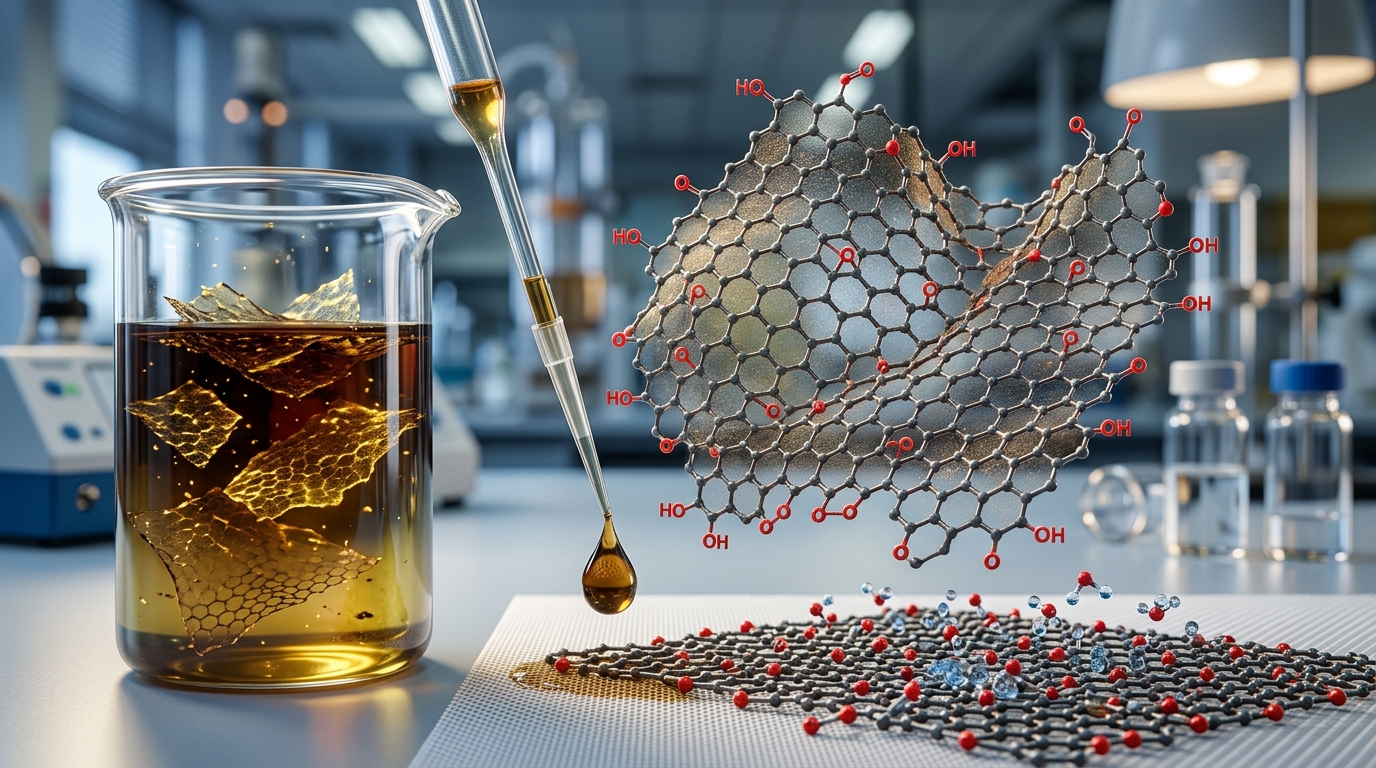
Graphene oxide is a chemically modified graphene derivative produced through the oxidative exfoliation of natural graphite. Its basal plane and edges are densely decorated with oxygen-containing functional groups, including hydroxyl, epoxy, and carboxyl groups. While these disruptions to the sp2 lattice render GO electrically insulating, they impart high dispersibility in water and polar solvents, making it a versatile precursor for coatings, membranes, and chemical synthesis.
4. Reduced Graphene Oxide (rGO)
Reduced graphene oxide is produced by subjecting graphene oxide to thermal, chemical, or electrochemical reduction to remove oxygen-containing groups. Although reduction partially restores electrical conductivity and aromatic structure, structural vacancies and residual heteroatoms remain. rGO provides a practical, powder-based alternative for energy storage electrodes and conductive additives where large volumes are required at moderate costs.
Synthesis and Production Methodologies
Graphene material manufacturing is broadly divided into two foundational engineering methodologies: bottom-up synthesis, which builds atomic lattices from molecular precursors, and top-down exfoliation, which separates bulk graphite into nanoscale sheets.
Bottom-Up Approaches
- Chemical Vapor Deposition (CVD): In standard thermal CVD, gaseous hydrocarbons (such as methane) are decomposed at elevated temperatures (typically 800°C to 1,000°C) over catalytic transition metal substrates, primarily copper or nickel. The dissolved or surface-adsorbed carbon nucleates and forms continuous single- or few-layer films. CVD produces the highest quality large-area sheets but requires delicate transfer steps to move the graphene onto non-metallic substrates.
- Epitaxial Growth: Graphene can be grown directly on crystalline silicon carbide (SiC) wafers by heating the substrate in high vacuum to sublime silicon atoms, leaving structured carbon layers behind. This technique avoids polymer transfer defects but relies on expensive substrates.
Top-Down Approaches
- Mechanical Exfoliation: The original method of cleaving bulk graphite using adhesive tape produces pristine, low-defect crystallites. While crucial for fundamental physics experiments, it yields minimal material and cannot be scaled industrially.
- Liquid-Phase Exfoliation (LPE): Bulk graphite is dispersed in tailored organic solvents, aqueous surfactant solutions, or ionic liquids, and subjected to high-shear mixing, microfluidization, or ultrasonication. The applied hydrodynamic shear forces overcome the interlayer van der Waals forces without significant chemical alteration, yielding unoxidized few-layer flakes.
- Chemical Exfoliation (Hummers' Method and Variants): Natural graphite flakes are treated with concentrated acids and strong oxidizing agents (e.g., sulfuric acid and potassium permanganate) to intercalate and oxidize the layers, creating water-dispersible graphene oxide that is subsequently exfoliated via mild agitation.
Key Industrial and Technological Applications
The versatility of graphene materials enables their integration across multiple industrial sectors, addressing specific mechanical, electrical, and transport challenges.
Advanced Composites and Structural Materials
Incorporating graphene nanoplatelets or functionalized graphene into polymers, concrete, and fiber-reinforced composites enhances mechanical durability, fatigue resistance, and dimensional stability. In thermoplastic and thermoset resins, low loadings (0.1% to 2% by weight) establish conductive networks that provide electrostatic discharge (ESD) protection, lightning strike shielding for aerospace components, and improved thermal management in structural housings.
Energy Storage: Batteries and Supercapacitors
Graphene materials serve multiple critical roles in next-generation electrochemical systems:
- Lithium-Ion and Sodium-Ion Batteries: Graphene conductive additives maintain electrical contact between active material particles throughout continuous charge-discharge expansion and contraction cycles. Graphene-silicon composite anodes mitigate mechanical pulverization, improving cycle life and charging rates.
- Supercapacitors: Due to its high theoretical specific surface area (up to 2,630 m2/g), pristine and porous graphene architectures facilitate high electric double-layer capacitance (EDLC), delivering high power densities and long operational lifespans.
Electronics, Sensors, and Photonics
While graphene's lack of an intrinsic electronic bandgap complicates its use in standard digital logic gates (such as general-purpose computer processors), its unique properties excel in analog, RF, and photonic systems:
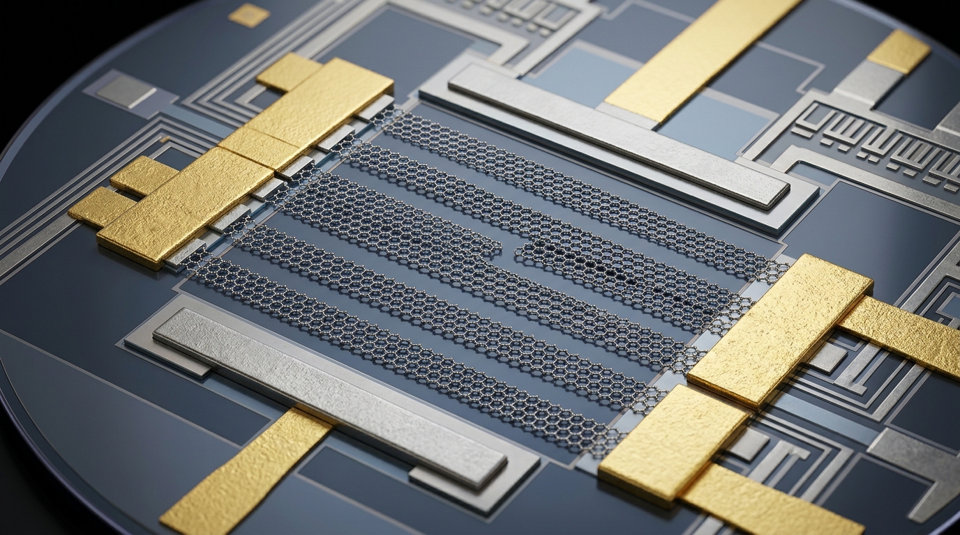
- High-Frequency Electronics: CVD graphene is deployed in low-noise amplifiers, radio-frequency mixers, and Hall-effect sensors operating in extreme temperature environments.
- Biosensors and Chemical Detection: The planar surface allows direct exposure of every atom to the environment. Target biomolecules or gas compounds binding to the surface induce measurable shifts in channel conductivity, enabling ultra-sensitive, real-time molecular diagnostics.
- Photodetectors: Graphene's ultra-broadband optical absorption and ultrafast carrier dynamics allow the fabrication of optical receivers operating across ultraviolet, visible, and infrared spectra.
Functional Coatings, Membranes, and Water Purification
Due to its chemical inertness and impermeability, graphene-infused coatings prevent corrosive agents (such as chloride ions and water) from reaching underlying metallic surfaces. In filtration, precisely engineered graphene oxide membranes allow selective water transport while blocking dissolved salts, heavy metal ions, and organic contaminants, establishing new possibilities for desalination and industrial effluent treatment.
Biomedical Technologies
In medical engineering, functionalized graphene derivatives are actively researched for targeted drug delivery carriers, tissue engineering scaffolds, and bio-compatible interfaces for neural recording. Graphene surfaces can support cell adhesion and proliferation while providing electrical stimulation to electroactive tissues, such as cardiac and neural cultures.
Commercialization Challenges and Standardization
Despite its proven technical advantages, the transition of graphene material from laboratory settings to commercial manufacturing faces clear operational, economic, and regulatory challenges.
Quality Standardization and Material Verification
A primary bottleneck in the early graphene market was the lack of standardized nomenclature and quality verification. Commercial powders labeled as "graphene" have historically ranged from high-purity few-layer flakes to ordinary graphite dust. The implementation of international standards, such as ISO/TS 80004-13, alongside systematic structural characterization—including Raman spectroscopy (ID/IG and 2D-band analysis), X-ray photoelectron spectroscopy (XPS), and atomic force microscopy (AFM)—is vital to establishing reliable supply chains.
Scalability and Defect Management
Scaling up production while maintaining rigorous structural consistency remains technically challenging. In top-down chemical processes, high yields often introduce lattice vacancies and functional defects that degrade electrical and thermal metrics. Conversely, large-area bottom-up CVD processes encounter difficulties in suppressing grain boundary defects, substrate wrinkling, and contamination during roll-to-roll mechanical transfer.
Dispersion and Interfacial Chemistry
Because pristine graphene surfaces are hydrophobic and interact strongly via van der Waals forces, graphene powders tend to agglomerate irreversibly when introduced into liquid resins, solvents, or matrix materials. Effective industrial deployment requires optimized surface functionalization, specialized surfactants, and high-energy mixing protocols to ensure uniform distribution and robust interfacial bonding with host materials.
Environmental, Health, and Safety (EHS) Considerations
As with all engineered nanomaterials, handling dry, respirable graphene powders requires specialized engineering controls, including HEPA filtration, local exhaust ventilation, and standard personal protective equipment (PPE). Research into the lifecycle toxicology, persistence, and environmental fate of graphene flakes indicates that biological impact is highly dependent on aspect ratio, lateral dimensions, surface charge, and agglomeration state. Industry guidelines prioritize liquid dispersions and masterbatches over loose powders to minimize inhalation exposure risks.
Summary and Realistic Outlook
Graphene material represents an exceptionally versatile class of two-dimensional nanostructures offering verified mechanical, electrical, and thermal properties. Rather than displacing established structural materials wholesale, graphene operates most effectively as an enabling additive and specialized functional component. As international standards mature and production costs decrease, high-purity CVD films and engineered graphene powders are continuing to establish dependable roles in microelectronics, composite engineering, energy systems, and protective coatings.