Graphene
Graphene is a single-atom-thick layer of carbon atoms arranged in a two-dimensional (2D) hexagonal honeycomb lattice. As the foundational building block for other graphitic materials—such as three-dimensional graphite, rolled one-dimensional carbon nanotubes, and zero-dimensional fullerenes—graphene represents the first isolated stable two-dimensional crystal known to material science. Its sp2-hybridized carbon network gives rise to an extraordinary combination of electrical conductivity, mechanical strength, thermal transport, and optical transparency.
The Discovery of Graphene
For decades, theoretical physicists believed that strictly two-dimensional atomic crystals could not exist in an isolated state because thermal fluctuations at room temperature would cause the lattice to curl or decompose. Although thin layers of graphite had been studied on various substrates since the mid-twentieth century, true monolayer graphene was not definitively isolated until 2004.
Physicists Andre Geim and Konstantin Novoselov at the University of Manchester isolated monolayer graphene using a deceptively simple technique known as micromechanical cleavage, or the “scotch tape method.” By repeatedly peeling standard adhesive tape against high-purity graphite and pressing the residue onto an oxidized silicon wafer, they isolated single-layer flakes thin enough to be optically identified and electrically measured. This breakthrough demonstrated that stable 2D crystals could exist under ambient conditions and earned Geim and Novoselov the Nobel Prize in Physics in 2010.
Core Physical and Chemical Properties
Graphene owes its extreme physical properties to the strength of its in-plane carbon-carbon σ-bonds and the delocalized π-electron cloud that extends perpendicular to the atomic plane.
1. Electrical Properties and Charge Carrier Mobility
Graphene is a zero-bandgap semimetal with linear electronic dispersion near the corners of its Brillouin zone (known as Dirac points). In this regime, electrons and holes behave as massless relativistic particles, or Dirac fermions. This unique band structure yields exceptionally high charge carrier mobility, exceeding 200,000 cm2/(V·s) in suspended samples at low temperatures, and routinely remaining above 15,000 cm2/(V·s) at room temperature on standard substrates. As a result, graphene conducts electricity with minimal resistive scattering.
2. Mechanical Strength and Elasticity
The sp2 hybridization of carbon atoms creates some of the strongest chemical bonds known. Defect-free monolayer graphene exhibits an intrinsic tensile strength of approximately 130 GPa and a Young’s modulus of roughly 1 TPa (one terapascal). This makes pristine graphene over a hundred times stronger than structural steel of equivalent thickness, while remaining lightweight and flexible enough to sustain elastic deformations of up to 20 percent without fracturing.
3. Thermal Conductivity
Heat conduction in carbon materials is dominated by acoustic phonons. In graphene, the strong covalent bonding and low atomic mass permit rapid vibrational transport. Pristine, suspended monolayer graphene demonstrates a room-temperature thermal conductivity between 3,000 and 5,000 W/(m·K), substantially outperforming bulk copper (~400 W/(m·K)) and standard graphite.
4. Optical Transparency
Despite being an atomic monolayer, graphene absorbs a measurable amount of incident white light. Its optical absorption is defined almost entirely by the fine-structure constant, absorbing roughly 2.3% of light across the visible spectrum while transmitting the remaining ~97.7%. This high optical transparency, paired with electrical conductivity, makes graphene an attractive candidate for transparent conductive surfaces.
Overview of Primary Synthesis Methods
The production method dictates the quality, flake size, defect density, and cost of the resulting graphene. Different commercial use cases require different manufacturing techniques.
Mechanical Exfoliation
Mechanical cleavage uses shear or normal forces (such as adhesive peeling) to separate van der Waals bonded layers from bulk graphite crystals. While this method yields the highest-quality, defect-free monolayer flakes ideal for fundamental physics research, it produces microscopic yields and cannot be scaled for industrial manufacturing.
Chemical Vapor Deposition (CVD)
Chemical vapor deposition involves heating a gaseous carbon precursor (such as methane) inside a reaction chamber until it dissociates on a catalytic metal substrate, typically copper or nickel foil. As the substrate cools, a continuous, large-area monolayer or few-layer graphene film forms on the surface. CVD is the primary method for producing continuous sheets for electronics, touchscreens, and transparent electrodes, though transferring the delicate film from metal to functional substrates remains a technical bottleneck.
Liquid-Phase Exfoliation (LPE)
In liquid-phase exfoliation, bulk graphite is dispersed in a specialized solvent or aqueous surfactant solution and subjected to ultrasonic energy or high-shear mixing. The cavitation forces overcome the interlayer van der Waals attraction, yielding suspensions of unfunctionalized graphene nanoplatelets (GNPs) and few-layer graphene. LPE is scalable and cost-effective for composite and coating additives, though the flakes are typically polydisperse in thickness and lateral size.
Reduction of Graphene Oxide (rGO)
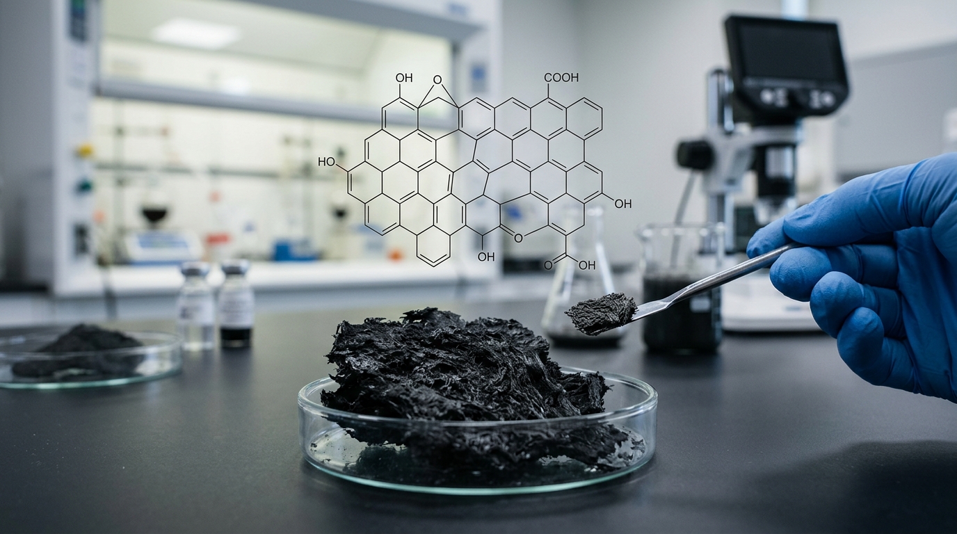
Chemical methods like the modified Hummers’ method treat graphite with strong oxidizing acids, producing graphene oxide (GO) decorated with hydroxyl, epoxide, and carboxyl functional groups. This oxidized form readily disperses in water. Subsequent chemical, thermal, or electrochemical treatment removes many of the oxygen groups to produce reduced graphene oxide (rGO). Although rGO retains residual structural defects and lower conductivity than pristine graphene, it offers high-volume throughput suitable for bulk structural composites and energy storage applications.
Comparison of Graphene Material Variants
The term “graphene” encompasses several distinct commercial material grades, each tailored to specific functional needs:
| Variant | Typical Thickness | Primary Production Method | Key Strengths | Common Industrial Uses |
|---|---|---|---|---|
| Monolayer CVD Graphene | 1 atomic layer (~0.34 nm) | Chemical Vapor Deposition | Highest transparency, exceptional carrier mobility, continuous sheet area | Sensors, high-frequency transistors, transparent electrodes |
| Graphene Nanoplatelets (GNPs) | 2 to 10+ nm (few to multi-layer) | High-shear / Liquid exfoliation | Low cost, high bulk thermal/electrical conductivity, easy blending | Polymer composites, conductive inks, thermal interface materials |
| Graphene Oxide (GO) | 1 to few layers (heavily oxidized) | Chemical oxidation of graphite | Hydrophilic, dispersible in water, easy chemical functionalization | Membranes, water purification, biomedical research coatings |
| Reduced Graphene Oxide (rGO) | 1 to few layers (partially restored) | Thermal/chemical reduction of GO | Scalable volume, restored electrical conductivity, porous structures | Battery electrodes, supercapacitors, anti-corrosion barriers |
Major Application Areas
Graphene’s versatile properties allow it to serve as a functional additive or primary substrate across several distinct industries.
1. Energy Storage and Battery Technology
In lithium-ion and sodium-ion batteries, graphene additives improve electrical transport throughout the electrode matrix. Adding small weight percentages of graphene nanoplatelets or rGO to cathode formulations (like lithium iron phosphate) improves electron transport and reduces internal resistance, facilitating faster charging rates and higher power densities. In supercapacitors, the high specific surface area of porous graphene structures allows for substantial electrostatic charge storage at the electrode-electrolyte interface.
2. Advanced Composite Materials
Incorporating graphene flakes into polymer resins, elastomers, and cementitious matrices enhances the mechanical durability, thermal dissipation, and barrier properties of bulk materials. In polymer engineering, low-loading additions of functionalized graphene increase elastic modulus and tensile strength without adding substantial weight. In construction, graphene-augmented concrete exhibits increased compressive strength and reduced porosity, which curbs moisture penetration and extends structural lifespans.
3. Electronics and High-Frequency Devices
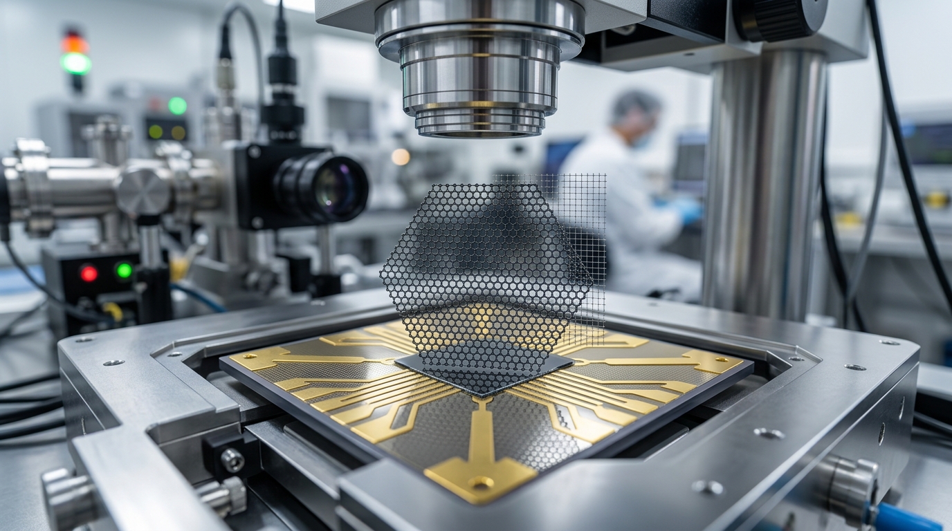
Because pristine graphene lacks an intrinsic electronic bandgap, it cannot naturally switch off like silicon in standard digital logic gates. However, its high electron mobility makes it well-suited for high-frequency analog electronics, radio-frequency (RF) transistors, Hall-effect magnetic sensors, and photodetectors capable of operating across broadband wavelengths from ultraviolet to terahertz frequencies.
4. Filtration, Desalination, and Barrier Membranes
Porous graphene sheets and stacked graphene oxide membranes offer sub-nanometer sieving channels. Because pristine graphene is impermeable to all standard gases and liquids (including helium), precisely engineered nanopores can separate specific salt ions, organic contaminants, or gas molecules while permitting rapid water transport. This enables energy-efficient reverse osmosis desalination and gas separation technologies.
5. Functional Coatings and Thermal Management
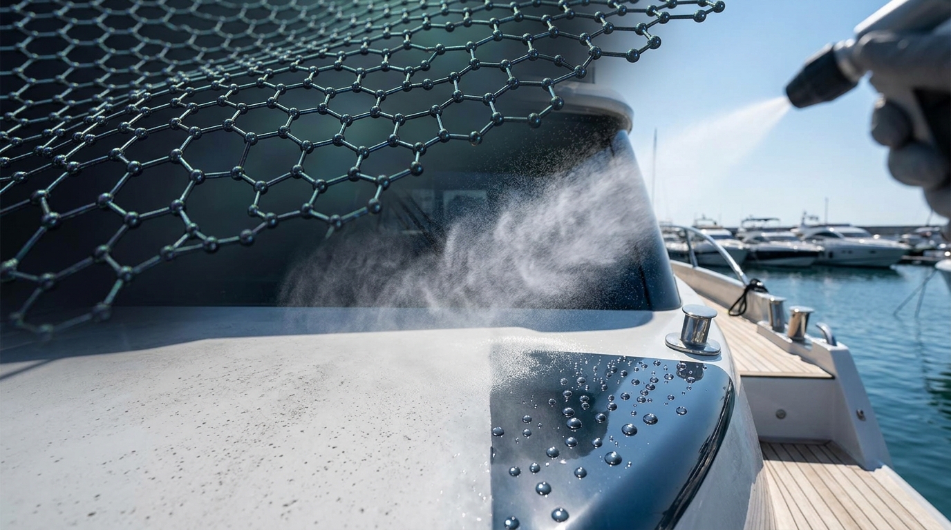
When integrated into liquid coatings, graphene creates a tortuous physical path that blocks corrosive agents like oxygen, moisture, and chloride ions from reaching underlying metallic surfaces. In electronics packaging, graphene-based thermal interface materials (TIMs) and heat-spreading films draw heat away from compact central processing units and power amplifiers to maintain operating efficiency.
Commercialization Challenges and Limitations
Despite significant laboratory validation, broad commercial deployment of graphene is constrained by several engineering, economic, and manufacturing bottlenecks:
- Scalability and Quality Consistency: Large-scale production techniques often yield materials with variable thickness, flake size distribution, and defect counts. Maintaining batch-to-batch consistency is an ongoing challenge for quality assurance in high-reliability industries.
- CVD Transfer Complications: While continuous CVD monolayer films can be grown on copper foils, detaching the atomic sheet and transferring it onto target substrates (such as silicon wafers or flexible polymers) frequently introduces wrinkles, tears, and chemical residues that degrade electronic performance.
- Absence of a Native Bandgap: Engineering a functional bandgap in graphene for digital logic typically requires structural modifications—such as cutting it into narrow nanoribbons or applying high electric fields to bilayer sheets—which drastically reduces charge carrier mobility and complicates fabrication.
- Agglomeration and Dispersion: In composite manufacturing, unfunctionalized graphene flakes tend to restack due to attractive van der Waals forces. Incomplete dispersion creates structural weak spots rather than reinforcing the host matrix.
- Cost vs. Performance Parity: In many mature applications, lower-cost carbon materials such as carbon black, synthetic graphite, and carbon fibers provide adequate performance. Graphene must deliver clear functional improvements to justify its higher raw material and processing costs.
Environmental and Lifecycle Considerations
Evaluating the lifecycle impact of graphene involves balancing synthesis footprints with performance gains during active use. Chemical oxidation methods (such as those used to produce graphene oxide) consume significant amounts of concentrated sulfuric acid, potassium permanganate, and rinsing water, requiring dedicated waste neutralization systems. In contrast, mechanical and shear-exfoliation techniques use milder reagents but demand substantial mechanical energy.
Over a full operational lifecycle, lightweighting automotive components or extending the operational lifespan of industrial infrastructure with graphene coatings can offset initial production footprints. Continued material science research focuses on refining green synthesis routes, including catalytic conversion of captured methane and biocarbon sources, to reduce the environmental footprint of large-scale manufacturing.
Summary Glossary of 2D Materials Terms
- 2D Material: A crystalline substance consisting of a single layer of atoms, where electrons are constrained to planar motion.
- Dirac Point: The point in the electronic band structure where conduction and valence bands meet linearly, causing electrons to behave as if they have zero effective mass.
- Exfoliation: The process of separating the layered sheets of a 3D layered crystal (like graphite) into thinner or single-layer forms.
- Graphene Nanoplatelet (GNP): A multi-layer graphene particle typically between 1 and 20 nanometers thick, used widely as a structural additive.
- sp2 Hybridization: The spatial bonding arrangement where one s-orbital and two p-orbitals mix to form three planar bonds oriented at 120-degree angles, creating a hexagonal network.