First Graphene
The isolation of the first graphene monolayer settled a decades-old debate in solid-state physics. Before researchers successfully extracted an individual, atom-thick sheet of carbon from bulk graphite, prevailing thermodynamic theory held that strictly two-dimensional crystals were inherently unstable and could not exist at room temperature. The practical demonstration that a stable, one-atom-thick hexagonal lattice could be isolated, manipulated, and electrically measured opened the field of two-dimensional nanomaterials and redefined modern condensed-matter research.
The Theoretical Barrier: Why 2D Crystals Were Thought Impossible
For more than half a century, theoretical physicists argued that a freestanding two-dimensional lattice was a mathematical curiosity rather than a physical reality. Foundational work by Rudolf Peierls and Lev Landau suggested that thermal fluctuations in a two-dimensional crystal would generate displacement amplitudes comparable to interatomic distances, causing the lattice to melt or disintegrate at any finite temperature. This concept was later formalized by the Mermin-Wagner theorem, which demonstrated that continuous symmetries cannot be spontaneously broken in one or two dimensions at non-zero temperatures.
Because of these thermodynamic constraints, experimentalists assumed that any isolated atomic sheet would immediately curl into zero-dimensional fullerenes, roll into one-dimensional carbon nanotubes, or collapse back into three-dimensional graphite. When graphite was cleaved, researchers expected to obtain microscopic multi-layer platelets at best, never a continuous, pristine monolayer.
What theoretical models had overlooked was that graphene avoids thermal destruction by microscopic warping. In reality, a freestanding sheet exhibits sub-nanometer out-of-plane ripples. These three-dimensional corrugations couple with in-plane acoustic phonons, stabilizing the overall two-dimensional framework without sacrificing the atomic integrity of the hexagonal lattice.
The Breakthrough: Micromechanical Cleavage
The realization of isolated single-layer carbon did not require ultra-expensive particle accelerators or complex molecular beam epitaxy. In 2004, physicists Andre Geim and Konstantin Novoselov at the University of Manchester isolated the first verified single-layer graphene using an elegant, deceptively simple technique known as micromechanical cleavage, colloquially known as the Scotch tape method.
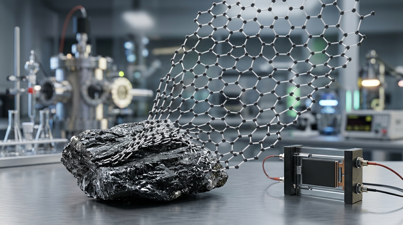
Graphite consists of graphene sheets stacked together via weak van der Waals interactions, with an interlayer binding energy of approximately 30 to 60 milli-electronvolts per atom. In contrast, the carbon atoms within each individual layer are joined by extremely strong $sp^2$ covalent bonds (carbon-carbon bond length of roughly 0.142 nanometers). This dramatic anisotropy in mechanical strength means that applying a transverse shear force can pull layers apart without rupturing the in-plane bonds.
The basic isolation process follows a systematic physical routine:
- Bulk Peeling: A small flake of highly oriented pyrolytic graphite (HOPG) or natural graphite is placed on ordinary adhesive tape.
- Iterative Thinning: Folding and peeling the tape repeatedly splits the graphite into progressively thinner flakes, overcoming interlayer van der Waals forces.
- Substrate Transfer: The adhesive tape carrying the cleaved fragments is pressed firmly against an oxidized silicon wafer and gently peeled away, leaving isolated flakes bound to the substrate by surface adhesion.
This achievement earned Geim and Novoselov the Nobel Prize in Physics in 2010. While the physical separation was simple in retrospect, the true scientific triumph lay in finding, identifying, and characterizing the isolated monolayers among thousands of thicker graphite fragments.
Proving Monolayer Thickness: The Four Diagnostic Pillars
Isolating a transparent, atom-thick sheet is useless if you cannot find it or prove its single-layer nature. The Manchester team solved the identification problem by exploiting an optical phenomenon on a precisely tuned substrate, followed by rigorous structural and electrical spectroscopy.
1. Optical Interference Contrast
A single layer of carbon absorbs only 2.3% of incident white light, making it virtually invisible on most surfaces. However, when deposited onto a silicon wafer topped with a silicon dioxide optical spacer of a specific thickness (typically 300 nanometers or 90 nanometers), an interference effect occurs. The minute optical path difference introduced by the single atomic layer alters the interference color of the reflected light under a standard optical microscope, making monolayer flakes visible as faint violet or pale blue silhouettes.
2. Atomic Force Microscopy (AFM)
Contact and tapping-mode atomic force microscopy measure surface topography with sub-nanometer vertical resolution. While the intrinsic thickness of a graphene layer within graphite is approximately 0.335 nanometers, AFM measurements of isolated graphene on silicon dioxide typically yield an apparent height between 0.4 and 1.0 nanometer. This apparent discrepancy stems from chemical contrast, trapped moisture, and differences in tip-sample electrostatic interactions between the carbon sheet and the underlying oxide.
3. Raman Spectroscopy
Raman spectroscopy serves as the definitive fingerprint for carbon allotropes. When monochromatic laser light interacts with the lattice vibrations (phonons) of the first graphene sheets, three primary features emerge:
- The G Band (~1580 cm⁻¹): Corresponds to the high-frequency in-plane optical phonon mode ($E_{2g}$) of $sp^2$ carbon atoms.
- The 2D Band (~2700 cm⁻¹): A second-order, two-phonon process highly sensitive to electronic band structure. In a true monolayer, the 2D band is a single, sharp, symmetric Lorentzian peak with an intensity substantially higher than the G band ($I_{2D} / I_G > 2$). In multilayer flakes, the 2D band broadens and splits into multiple overlapping components.
- The D Band (~1350 cm⁻¹): A defect-activated breathing mode of six-membered rings. In high-quality pristine flakes, the D band is essentially absent, confirming an intact crystal lattice.
4. The Half-Integer Quantum Hall Effect
The definitive proof of graphene’s unique two-dimensional nature came from low-temperature magnetotransport measurements. When placed in strong magnetic fields, the charge carriers in pristine monolayer flakes exhibited an unconventional half-integer quantum Hall effect. This behavior confirmed that the charge carriers were not standard Schrödinger electrons with effective mass, but massless Dirac fermions governed by relativistic quantum mechanics.
The Electronic Properties Unveiled by the First Flakes
The initial characterization of mechanically exfoliated flakes revealed electronic properties distinct from conventional metals and semiconductors. The honeycomb carbon lattice gives rise to conical energy bands intersecting at the corners of the first Brillouin zone—points known as Dirac cones.
At these intersection points, energy varies linearly with momentum ($E = ħ v_F k$), meaning the electrons travel at an effective Fermi velocity ($v_F$) of roughly $10^6$ meters per second, about 1/300th the speed of light. Because the conduction and valence bands touch with zero bandgap, graphene behaves as a zero-gap semimetal.
These initial flakes demonstrated an ambipolar electric field effect: adjusting an external gate voltage continuously shifted the Fermi level between the conduction and valence bands, allowing researchers to switch charge carriers smoothly between electrons and holes with continuous modulation of carrier concentrations up to $10^{13} text{ cm}^{-2}$. Furthermore, room-temperature electron mobilities exceeded $15,000 text{ cm}^2/(text{V}cdottext{s})$, outperforming commercial silicon by an order of magnitude even on rough, unpassivated substrates.
Original Flakes vs. Scaled Production Methods
The micromechanical cleavage technique used to produce the first graphene yielded the highest crystalline perfection ever achieved. However, because it produces small, randomly distributed flakes ranging from a few microns to fractions of a millimeter, it cannot support industrial-scale manufacturing. Subsequent research developed alternative synthesis routes, each presenting specific engineering tradeoffs.
| Synthesis Method | Crystalline Quality | Typical Flake Size | Primary Tradeoff / Limitation | Primary Application |
|---|---|---|---|---|
| Mechanical Exfoliation (Tape) | Pristine (No structural defects) | Microns to ~1 mm | Extremely low throughput; manual process | Fundamental physics research, prototype devices |
| Chemical Vapor Deposition (CVD) | Polycrystalline with grain boundaries | Wafer-scale to continuous rolls | Transfer residue, metallic substrate contamination | Transparent conductors, high-frequency electronics |
| Liquid-Phase Exfoliation (LPE) | Good (Few basal plane defects) | 100 nm to tens of microns | Mixture of monolayer and few-layer flakes | Conductive inks, battery electrodes, composites |
| Oxidation-Reduction (rGO) | Disrupted lattice with residual oxygen | Sub-micron to microns | Reduced electrical conductivity and structural strength | Water filtration membranes, structural additives |
Common Misconceptions Regarding the First Isolation
Several persistent historical and technical myths surround the initial isolation of graphene:
- Misconception: Graphene had never been observed prior to the Manchester experiment. Transmission electron microscopists had observed thin carbon sheets resting on metallic grids or grown epitaxially on silicon carbide decades prior. However, those samples were either tightly bound to a supporting substrate, heavily degraded by oxidation, or impossible to isolate and measure electrically. The milestone lay in isolating freestanding, identifiable single layers on a dielectric surface ready for device fabrication.
- Misconception: The discovery was purely an accidental stroke of luck. While the Scotch tape approach was developed during open-ended experimental trials (“Friday evening experiments”), the ability to recognize sub-nanometer optical shifts on silicon dioxide, design lithographic contacts, and confirm relativistic transport required sophisticated solid-state physics and systematic validation.
- Misconception: All commercial materials labeled “graphene” behave like the first flakes. Modern bulk additives often consist of multi-layer graphene nanoplatelets (5 to 40 layers) or chemically modified graphene oxide. These materials offer practical mechanical and thermal benefits to bulk matrices, but they lack the pristine ballistic transport, massless Dirac fermion dispersion, and quantum Hall characteristics of true single-layer graphene.
The Durable Impact on Materials Science
The realization of the first graphene demonstrated that two-dimensional atomic crystals are physically viable and chemically robust. This breakthrough dismantled thermodynamic assumptions and triggered the discovery of an entire family of 2D materials, including hexagonal boron nitride, transition metal dichalcogenides (such as molybdenum disulfide), and MXenes. By proving that single-atom layers could be extracted, handled, and harnessed, the first graphene established a foundational platform for modern nanoscale electronics, surface chemistry, and layered van der Waals heterostructures.