How Is Graphene Made?
Graphene is produced through two distinct engineering pathways: top-down exfoliation, which separates the stacked atomic sheets of natural or synthetic graphite, and bottom-up growth, which synthesizes single-atom-thick carbon lattices directly from carbon-containing gases or small organic molecules. The chosen manufacturing method dictates the resulting material’s physical structure, defect density, sheet dimensions, and electrical performance.
Understanding how graphene is made requires looking past the idea of a single uniform substance. A manufacturer creating conductive additives for concrete requires kilograms of thick, dispersible flakes, whereas a semiconductor fabricator requires a continuous, defect-free monolayer film spanning an entire silicon wafer. Each method solves a different engineering challenge with distinct trade-offs in purity, scalability, and cost.
The Two Primary Manufacturing Philosophies
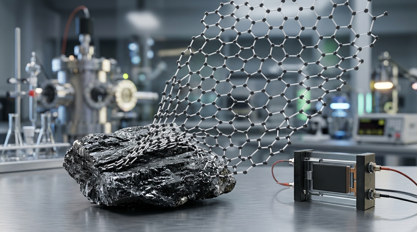
Graphite consists of millions of individual graphene sheets stacked together like a ream of paper. Within each individual sheet, carbon atoms are bonded tightly by strong covalent bonds into a hexagonal honeycomb lattice. Between the sheets, however, only weak van der Waals forces hold the layers together.
Top-down methods use physical, chemical, or electrochemical energy to overcome these weak interlayer attractions without tearing the strong carbon-to-carbon bonds within the plane. Bottom-up methods operate on the opposite principle: they dissociate carbon-rich precursor molecules into free carbon radicals, which then assemble spontaneously into hexagonal lattices on a supporting surface.
Top-Down Manufacturing Methods
Top-down processes produce powders, flakes, platelets, and liquid dispersions. These formats are primarily used in structural composites, thermal interface materials, conductive coatings, energy storage electrodes, and functional masterbatches.
1. Mechanical Exfoliation (Micromechanical Cleavage)
Historically demonstrated in 2004 using common adhesive tape to repeatedly peel layers from highly oriented pyrolytic graphite, mechanical exfoliation isolates pristine, single-layer graphene crystals. When the tape is pressed onto graphite and peeled away, the adhesive forces exceed the interlayer van der Waals bonding.
Transferring the peeled remnants onto a silicon dioxide substrate yields isolated flakes of exceptional structural integrity. Because no aggressive chemicals or high temperatures are involved, mechanically exfoliated graphene exhibits theoretical electron mobility and minimal crystal defects. However, the process yields only microscopic flakes measuring tens of micrometers, making it an indispensable tool for fundamental laboratory physics but completely unviable for commercial manufacturing.
2. Liquid-Phase Exfoliation (LPE)
Liquid-phase exfoliation scales the physical separation of graphite by immersing it in a liquid medium and applying intense hydrodynamic shear forces, ultrasonic cavitation, or microfluidization. When acoustic or shear energy travels through the liquid, it creates microscopic vacuum bubbles that collapse violently against the graphite particles, wedging the atomic layers apart.
To prevent the freshly stripped graphene sheets from re-aggregating, the liquid must match the surface energy of graphene. Manufacturers use specialized organic solvents like N-methyl-2-pyrrolidone (NMP) or water combined with ionic or non-ionic surfactants. Liquid-phase exfoliation produces unoxidized, high-conductivity flakes with minimal lattice damage, making the resulting suspensions ideal for printed electronics, conductive inks, and battery slurry additives.
3. Chemical Oxidation and Reduction (The Hummers Route)
The most common industrial method for producing bulk graphene derivatives involves aggressively oxidizing raw graphite powder using concentrated sulfuric acid, sodium nitrate, and potassium permanganate. This chemical treatment intercalates oxygen-containing functional groups—such as epoxy, hydroxyl, and carboxyl groups—into the graphite galleries.
These oxygen groups widen the interlayer spacing and make the material hydrophilic, allowing complete separation into single sheets in water via mild agitation. The intermediate product is graphene oxide (GO), an electrical insulator due to disrupted electronic conjugation. To restore electrical and thermal conductivity, manufacturers apply chemical reducing agents (such as hydrazine or ascorbic acid), thermal annealing, or ultraviolet irradiation to create reduced graphene oxide (rGO).
While rGO can be manufactured in metric-ton quantities at accessible prices, the reduction process never fully repairs the carbon lattice. Residual oxygen atoms and structural vacancies remain, meaning rGO has lower electrical and thermal conductivity than pristine graphene.
4. Electrochemical Exfoliation
Electrochemical exfoliation drives charged ionic species between graphite layers using an electrical potential. A solid graphite rod or foil acts as the working electrode inside an electrolyte bath containing sulfate, perchlorate, or ionic liquid compounds.
When voltage is applied, ions migrate into the graphite galleries (intercalation). The simultaneous electrolysis of the solvent generates localized gases like sulfur dioxide or oxygen, which expand rapidly and push the graphene sheets apart. This method operates at room temperature, takes minutes rather than days, generates fewer lattice defects than wet chemical oxidation, and avoids toxic reducing agents.
Bottom-Up Manufacturing Methods
Bottom-up synthesis targets large-area, continuous, highly uniform films required for transparent touch displays, high-frequency transistors, photonics, and barrier membranes.
1. Chemical Vapor Deposition (CVD)
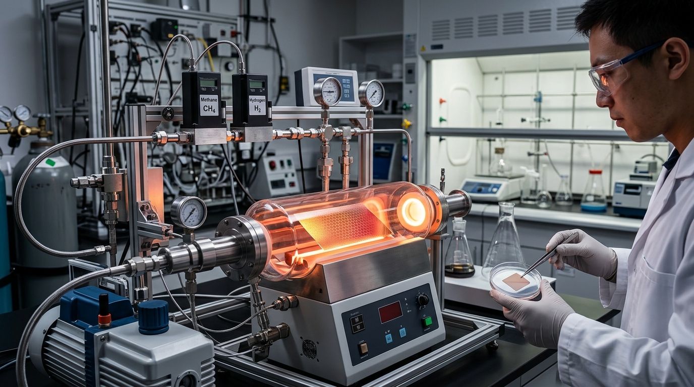
Chemical vapor deposition represents the standard industrial pathway for producing high-quality, continuous graphene films over large surface areas. In a typical low-pressure or atmospheric CVD furnace, a metal substrate (predominantly high-purity copper or nickel foil) is heated to temperatures between 800 and 1050 degrees Celsius.
A hydrocarbon precursor gas, typically methane mixed with hydrogen and argon, flows across the hot metal catalyst:
- Catalytic Dissociation: The heated metal surface breaks the carbon-hydrogen bonds in methane, releasing hydrogen gas and leaving active carbon atoms adsorbed on the surface.
- Surface Growth: On copper, carbon has extremely low solubility. Growth occurs exclusively on the surface, automatically halting once a single layer covers the copper (a self-limiting mechanism). On nickel, carbon dissolves into the metal bulk at high temperatures and precipitates onto the surface during cooling, which often forms multi-layer regions unless cooling rates are strictly controlled.
- Domain Coalescence: Individual graphene nucleation islands grow outward until they merge into a continuous polycrystalline film.
Roll-to-roll CVD systems produce continuous rolls of graphene on wide copper foils. While CVD yields high-purity films, the resulting sheets contain grain boundaries where different crystal domains meet, which slightly reduces mechanical strength and charge carrier mobility compared to single-crystal specimens.
2. Epitaxial Growth on Silicon Carbide (SiC)
Epitaxial growth produces wafer-scale graphene directly on a semiconducting platform without requiring metallic catalysts. High-purity silicon carbide wafers are heated to extreme temperatures exceeding 1200 to 1400 degrees Celsius under ultra-high vacuum or an inert argon atmosphere.
Because silicon has a much higher vapor pressure than carbon, silicon atoms selectively sublimate (evaporate) from the surface. The remaining carbon atoms spontaneously reorganize into an ordered graphene lattice matching the crystal symmetry of the underlying SiC substrate. Epitaxy eliminates the need to transfer the graphene layer onto a dielectric support, making it well-suited for radio-frequency electronic devices, quantum metrology standards, and high-speed communications.
3. Direct Laser Conversion and Flash Joule Heating
Alternative bottom-up and hybrid synthesis methods bypass traditional furnaces entirely:
- Laser-Induced Graphene (LIG): A commercial carbon dioxide or infrared laser irradiates specific polymers, such as polyimide, photothermally breaking chemical bonds and re-forming the carbon backbone into porous, three-dimensional graphene patterns in ambient air.
- Flash Joule Heating: Passing an intense electrical current through inexpensive carbonaceous materials (such as biochar, carbon black, or processed municipal solid waste) for milliseconds raises temperatures above 2700 degrees Celsius. This rapid pulse vaporizes non-carbon elements and stitches the carbon into turbostratic graphene, where layers are misaligned and easily separated without chemical additives.
The Substrate Transfer Challenge
For CVD graphene, synthesis is only the first step. Because the graphene is grown on metal foil, it must be removed and placed onto functional substrates like silicon, glass, or flexible polymers without tearing, wrinkling, or contaminating the single-atom layer.
In standard wet-transfer protocols, a protective polymer layer, usually poly(methyl methacrylate) (PMMA), is spin-coated over the graphene surface. The underlying copper is chemically dissolved in an acid or iron chloride bath, leaving the PMMA-graphene membrane floating on water. This film is scooped onto the target substrate, and the PMMA support is dissolved using acetone.
Transfer remains a significant source of defects in commercial production. Trapped solvent residue, structural wrinkles, micro-cracks, and chemical contamination during the etch step can degrade the electrical properties of the transferred film. Dry roll-to-roll lamination techniques using thermal release tapes or electro-delamination (which preserves and reuses the copper substrate) are increasingly replacing wet-chemical etching in high-throughput facilities.
Comparison of Graphene Production Techniques
| Manufacturing Method | Primary Product Form | Structural Quality | Throughput / Scalability | Common Commercial Target |
|---|---|---|---|---|
| Mechanical Exfoliation | Isolated mono/few-layer flakes | Pristine (No defects) | Extremely Low | Academic research, physics prototypes |
| Liquid-Phase Exfoliation | Dispersed pristine nanosheets | High (Low defects) | Medium to High | Conductive inks, composite resins, battery slurries |
| Chemical Oxidation (rGO) | Reduced oxide powders/pastes | Moderate (Defect-rich) | Very High (Tons) | Concrete additives, anti-corrosion paints, supercapacitors |
| Chemical Vapor Deposition | Continuous monolayer films | Very High (Polycrystalline) | High (Roll-to-roll) | Touch panels, optical sensors, transparent electrodes |
| SiC Epitaxy | Wafer-scale uniform layers | High (Substrate-coupled) | Low to Moderate | Quantum resistance standards, high-frequency electronics |
Quality Verification: How Manufacturers Test Graphene
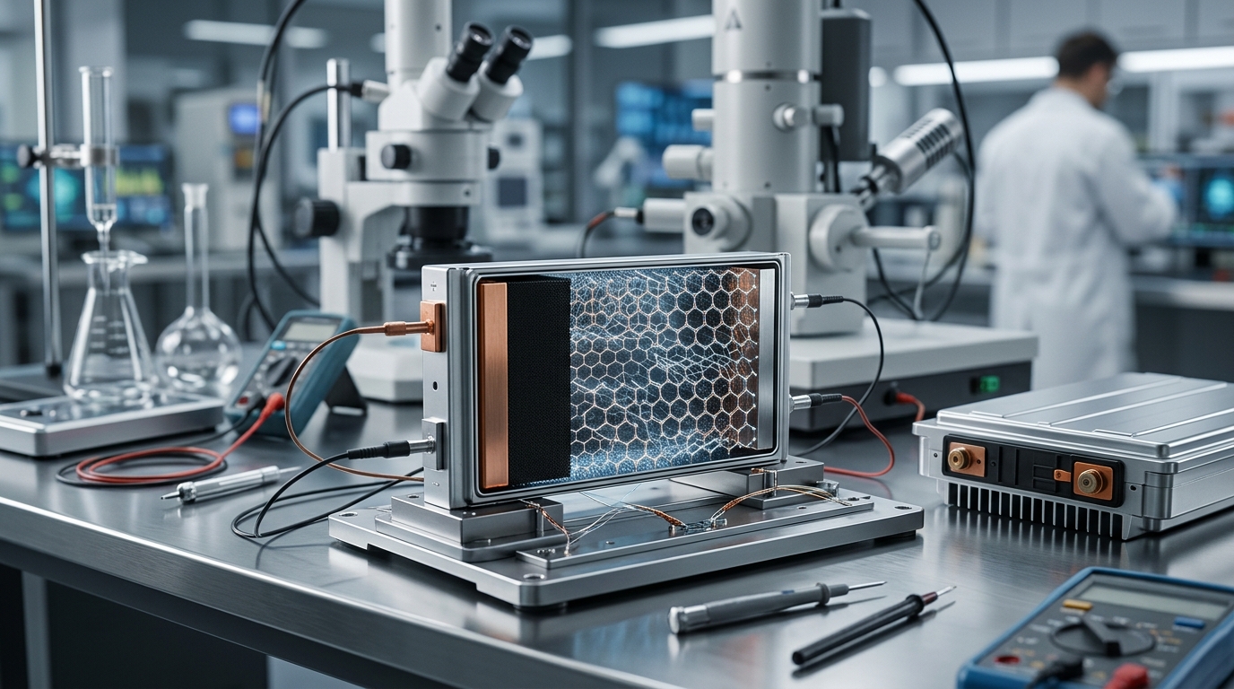
Because carbon powders can be easily mislabeled, international standards organizations define true graphene as containing between one and ten atomic layers. Industrial producers use specialized material characterization tools to confirm layer thickness, structural purity, and electrical performance:
- Raman Spectroscopy: The primary non-destructive test for carbon materials. Raman spectroscopy uses laser excitation to measure three key peaks: the D peak (showing crystal defects and edge boundaries), the G peak (representing in-plane carbon hybridization), and the 2D peak (revealing exact layer thickness and electronic band structure). A sharp, symmetric 2D peak twice the height of the G peak indicates single-layer graphene.
- Atomic Force Microscopy (AFM): Measures topological height down to the sub-nanometer scale, providing absolute verification of single-layer thickness (roughly 0.34 to 0.8 nanometers depending on substrate interaction).
- Transmission Electron Microscopy (TEM): High-resolution TEM images the hexagonal atomic arrangement directly and counts layer stacking at edge folds.
- Four-Point Probe Testing: Measures the sheet resistance of continuous films to ensure electrical continuity across square meters of transferred material.
Classification Boundaries and Industrial Terminology
In commercial supply chains, materials marketed as