Graphene Structure
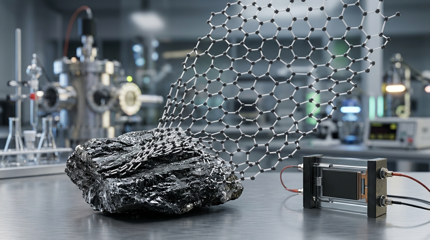
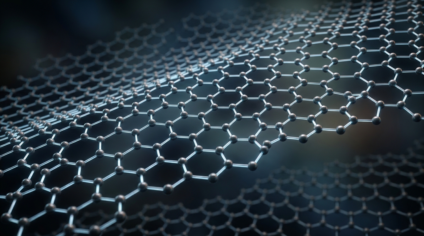
At its fundamental level, the graphene structure is an atomically thin, two-dimensional sheet composed entirely of carbon atoms arranged in a regular, repeating hexagonal pattern. Often described as atomic-scale chicken wire, this planar network represents the fundamental building block for all other graphitic allotropes, including zero-dimensional fullerenes, one-dimensional carbon nanotubes, and three-dimensional stacked graphite. The elegance of its atomic architecture is directly responsible for graphene’s benchmark thermal conductivity, exceptional mechanical strength, optical transparency, and unique electronic behavior.
The Atomic Architecture: Hybridization and Bonding
To understand the stability and behavior of graphene, one must examine how carbon atoms configure their electrons within the plane. Carbon has an atomic number of six, with an electron configuration of 1s² 2s² 2p². In the planar sheet of graphene, each carbon atom undergoes sp2 hybridization, combining its 2s orbital with two of its 2p orbitals (specifically, the 2px and 2py orbitals).
This hybridization yields three equivalent planar hybrid orbitals oriented at 120-degree angles to one another. When adjacent carbon atoms bond, these orbitals overlap head-on to establish strong covalent in-plane sigma bonds. The carbon-carbon bond length in pristine graphene is approximately 0.142 nanometers (1.42 Ångströms), slightly shorter than the single covalent bond found in diamond (0.154 nanometers). These rigid covalent bonds generate a robust backbone, endowing the monolayer with an intrinsic tensile strength of roughly 130 gigapascals and a Young’s modulus near 1 terapascal.
The remaining unhybridized orbital, the 2pz orbital, extends perpendicular to the planar sheet above and below the atomic core. These out-of-plane orbitals overlap laterally with those of neighboring carbon atoms to form a network of pi (π) bonds. The resulting delocalized pi electron cloud extends across the entire sheet. Because these π electrons are free to move across the lattice without being tied to specific atomic nuclei, they dictate graphene’s remarkable electrical conduction, optical properties, and chemical reactivity.
Lattice Geometry and Crystallography
Crystallographically, the honeycomb geometry of graphene is not a standard Bravais lattice because a single translation vector cannot generate every vertex of the hexagon. Instead, it is classified as a triangular Bravais lattice with a basis of two identical carbon atoms per unit cell, commonly designated as sublattices A and B.
This arrangement can be viewed as two interpenetrating triangular sublattices shifted relative to one another. Each atom belonging to sublattice A is surrounded by three nearest neighbors belonging to sublattice B, and vice versa. The lattice constant—the distance between identical repeating points in the triangular lattice—is approximately 0.246 nanometers (2.46 Ångströms).
In reciprocal space, which crystallographers and physicists use to map wave vectors and electron momentum, the Brillouin zone of graphene forms a hexagon. The corners of this hexagonal Brillouin zone, designated as the K and K’ points, represent the energy states where the valence and conduction bands intersect. The equivalence and symmetry between these two distinct valleys give rise to graphene’s valley degeneracy, a key parameter in advanced quantum electronic research.
Electronic Band Structure and Dirac Cones
The specific spatial symmetry of the honeycomb lattice governs how electrons propagate through graphene. In conventional semiconductor materials like silicon or gallium arsenide, the relationship between an electron’s energy and its momentum is parabolic (quadratic), meaning the electron behaves as a classical particle with an effective mass determined by the crystal lattice.
In graphene, however, the intersection of the π (bonding) and π* (antibonding) bands occurs precisely at the Fermi level at the six high-symmetry corners of the Brillouin zone. Near these points, the electronic energy exhibits a linear dispersion relation. The conical energy surfaces that touch at these points are known as Dirac cones, and the crossing points are called Dirac points.
Because energy is linearly proportional to momentum near the Dirac points, charge carriers in pristine graphene behave not as standard Schrödinger electrons, but as relativistic massless Dirac fermions. They travel through the crystal lattice at a Fermi velocity of approximately 10⁶ meters per second—roughly 1/300th the speed of light. This linear dispersion eliminates low-energy backscattering in pristine sheets, enabling room-temperature carrier mobilities exceeding 15,000 cm²/(V·s) on standard substrates and well over 200,000 cm²/(V·s) in suspended or boron-nitride-encapsulated configurations.
Because the valence and conduction bands touch without overlapping or creating an energy gap, pristine graphene is formally classified as a zero-bandgap semiconductor or a semimetal. While this allows rapid electron transport, the absence of an intrinsic bandgap presents an engineering challenge for digital logic transistors, which require an on/off current switching ratio that pristine planar graphene cannot provide naturally.
Edge Geometries: Armchair vs. Zigzag
When a finite sheet or narrow ribbon of graphene is cut, the boundaries terminate in specific geometric configurations that fundamentally alter local electronic states. The two primary crystallographic edge types are armchair and zigzag orientations, named after the profile of the carbon boundary.
- Armchair Edges: In this configuration, the boundary forms a repeating step pattern resembling the arms of an armchair. Armchair graphene nanoribbons exhibit width-dependent energy gaps due to quantum confinement and edge boundary conditions, transitioning between semiconducting states with varying bandgap magnitudes and metallic behavior.
- Zigzag Edges: In this profile, the edge is formed by a continuous line of carbon atoms alternating up and down. Zigzag terminations feature localized non-bonding edge states right at the Fermi energy. These edge states demonstrate localized magnetic polarization and higher chemical reactivity compared to the inert basal plane.
In practical material synthesis, edges are rarely purely armchair or zigzag; they typically consist of disordered, mixed boundaries with structural roughness that scatters electrons and broadens spectroscopic signatures.
Structural Defects in the Real Lattice
While theoretical models often assume an infinite, defect-free sheet, synthesized graphene—whether produced via chemical vapor deposition (CVD) or chemical exfoliation—contains structural deviations that modify its mechanical integrity, chemical affinity, and electrical transport.
Point Defects and Topological Rearrangements
Vacancies occur when one or more carbon atoms are missing from the crystal matrix. A monovacancy leaves three dangling bonds, which often undergo a Jahn-Teller reconstruction to form a five-membered ring and one dangling bond. Divacancies, where two adjacent atoms are missing, typically reconstruct into pairs of pentagons and octagons without leaving uncoordinated bonds.
A Stone-Wales defect is a purely topological rearrangement that involves no missing or added atoms. Instead, a 90-degree rotation of a single carbon-carbon bond transforms four adjacent hexagons into two pentagons and two heptagons (a 5-7-7-5 defect). This structural change introduces local out-of-plane strain and serves as a site for increased chemical functionalization.
Grain Boundaries and Wrinkling
Large-area graphene grown by CVD on metallic foils is polycrystalline. As individual graphene islands grow and coalesce, they meet at misoriented angles, creating one-dimensional grain boundaries composed of alternating pentagonal and heptagonal carbon rings. These grain boundaries act as scattering centers for electrons and phonons, reducing overall electrical mobility and thermal conductivity compared to single-crystal domains.
Furthermore, because two-dimensional membranes are thermodynamically unstable against thermal fluctuations without out-of-plane distortion, free-standing and supported graphene sheets exhibit intrinsic ripples and nanoscale wrinkles. These structural corrugations modify local hybridization from pure sp2 toward sp3 character, slightly altering local chemical reactivity.
Layer Stacking: Monolayer, Bilayer, and Beyond
Graphene is strictly defined as a single atom-thick sheet. However, multi-layer arrangements exhibit distinct physics depending on the number of layers and their geometric alignment.
Bernal vs. Non-Bernal Stacking
In bilayer graphene, the most common thermodynamically stable configuration is Bernal stacking (AB stacking). In this geometry, half of the carbon atoms in the upper layer sit directly over the center of a hexagon in the lower layer, while the other half sit directly over carbon atoms in the lower layer. This interlayer interaction breaks the inversion symmetry of the isolated monolayer, transforming the linear Dirac dispersion into a parabolic band structure with non-zero effective mass.
When an external perpendicular electric field is applied across an AB-stacked bilayer, it breaks the electrostatic potential balance between the top and bottom sheets, opening a controllable bandgap of up to a few hundred millielectronvolts—a feature absent in single-layer graphene.
Twisted Bilayers and Moiré Superlattices
When two graphene layers are stacked with an intentional rotational offset rather than strict AB alignment, they generate a geometric interference pattern known as a moiré superlattice. At a specific rotational misalignment near 1.1 degrees (the "magic angle"), the interlayer electron interactions cause the electronic band structure to flatten dramatically.
In these flat bands, the kinetic energy of electrons approaches zero relative to their mutual Coulomb interactions. This structural configuration gives rise to strongly correlated electron states, enabling unconventional superconductivity and correlated insulating behavior in an all-carbon system without heavy metal elements.
Structure-Property Relationships
Every major performance metric of graphene originates directly from its crystallographic and orbital properties, as detailed in the matrix below:
| Structural Feature | Physical Mechanism | Resulting Material Property |
|---|---|---|
| Covalent sp2 σ-bonds | Short, stiff carbon-carbon bonds (1.42 Å) in a planar network | Tensile strength (~130 GPa), high Young’s modulus (~1 TPa) |
| Delocalized π-electron cloud | Unconfined out-of-plane pz orbital overlap across the lattice | High electrical conductivity and optical absorption (~2.3% per sheet) |
| Two-sublattice honeycomb symmetry | Band crossing at Dirac points producing linear dispersion (E ∝ k) | Massless Dirac fermion behavior, ultrahigh carrier mobility |
| Stiff lattice vibrations (phonons) | High sound velocity and long mean free path of acoustic phonons | High in-plane thermal conductivity (3,000–5,000 W/m·K) |
| Single-atom thickness (0.335 nm equivalent) | Complete exposure of all constituent atoms on the surface | Theoretical specific surface area of 2,630 m²/g |
Historical Characterization Context
Although theoretical studies of a single graphitic layer date back to mid-twentieth-century solid-state physics, graphene was long thought to be thermodynamically unstable in an isolated free state. The field shifted permanently in 2004 when researchers successfully isolated monolayer flakes from bulk graphite using micromechanical cleavage (the scotch-tape method) on oxidized silicon wafers.
This experimental breakthrough demonstrated that the two-dimensional lattice could exist stably at ambient conditions due to microscopic out-of-plane rippling, which lowers total free energy. Subsequent structural confirmations using high-resolution transmission electron microscopy (HRTEM), atomic force microscopy (AFM), and Raman spectroscopy confirmed the exact atomic spacings and vibrational signatures predicted by quantum mechanics.
Practical Implications for Material Integration
Understanding the precise geometry of graphene is essential for translating its laboratory performance into industrial applications. Because every atom is a surface atom, any environmental contamination, substrate roughness, or chemical functionalization directly influences the electronic and physical properties of the lattice.
When integrating graphene into composite matrices, the pristine, chemically inert basal plane often requires controlled structural modification—such as oxidation to form graphene oxide—to improve dispersion and interfacial bonding with polymers or ceramics. Conversely, high-speed electronic and optoelectronic devices require unfunctionalized, single-crystal, continuous lattices on flat dielectric substrates to preserve linear dispersion and minimize scattering from grain boundaries and point defects.
By mapping and controlling the atomic framework—from bond lengths and defect concentrations to edge types and stacking angles—materials scientists can tailor the graphene structure precisely to meet the demands of thermal management, structural composites, barrier membranes, and high-frequency electronics.