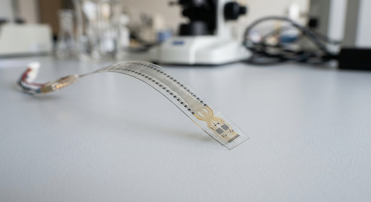
Adisyn says it has made a low-temperature graphene layer for semiconductor interconnects
Adisyn said on April 20, 2026, that it had demonstrated a continuous graphene layer on a 1-centimeter coupon using industrial atomic layer deposition equipment, a development the company is framing as a step toward semiconductor interconnect use. The result matters because graphene has long promised speed and conductivity advantages in chips, but only if it can be deposited within the temperature and tooling constraints of existing fabrication lines.
Low-temperature deposition is the point of the announcement
The company said the graphene film was grown on standard industrial ALD equipment and that the process stayed below the thermal ceiling typically acceptable in semiconductor manufacturing. That is the central news value here: not graphene itself, but a deposition route intended to work inside current chipmaking workflows rather than require a separate production stack.
Adisyn described the result as a continuous layer on a 1-centimeter coupon, which is still a small test sample rather than a production wafer. Even so, it is a more operationally relevant benchmark than isolated laboratory results because it speaks to repeatability, film continuity and compatibility with fab tools.
Why interconnects are the commercial target
The company is pursuing semiconductor interconnects, the wiring layers that move signals between device elements on a chip. Those paths face growing performance pressure as chip geometries shrink, and graphene has been widely studied as a possible materials platform for reducing resistance and improving thermal behavior.
That is also where the commercialization challenge has been most stubborn. A promising material can remain commercially irrelevant if it cannot be formed at scale, at low temperature and without disrupting established process lines. Adisyn’s announcement is aimed squarely at that barrier.
A small process milestone, not a finished product
The result does not mean graphene interconnects are ready for mass production. The remaining questions are the ones that decide whether a materials announcement becomes a manufacturing program: wafer-scale uniformity, defect control, process yield, device reliability and integration with the rest of the chip stack.
Still, the April 20 demonstration gives the graphene semiconductor field a fresh data point at a time when many claims remain aspirational. The immediate significance is practical: a low-temperature route on industrial equipment is the kind of milestone chipmakers can actually evaluate, even if commercialization remains a longer test.
Source: GrapheneUses.org
Date: 2026-04-24