Nature Communications study shows a faster route to twisted 2D semiconductor stacks
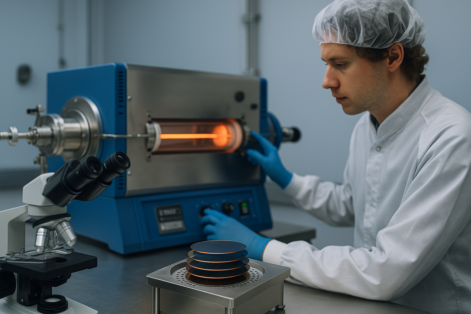
Researchers have reported a new way to grow twisted two-dimensional semiconductor heterostructures with more control over the angle between layers, a long-standing bottleneck for moiré materials used in optics, electronics and quantum devices. The study, published April 13, 2026, in Nature Communications, describes a heating-rate-controlled chemical vapor deposition process for transition metal dichalcogenide stacks.
Heating rate becomes the control knob
Instead of relying on conventional isothermal growth, the method uses the ramp-up stage of the furnace to guide epitaxial formation. The authors found that a low heating rate of 10 C per minute favored twist angles at or below 22.5 degrees, while rates of 30 C per minute or higher promoted angles of 30.0 degrees and above.
In total, the team reported 18 twisted transition metal dichalcogenide heterostructures made through the approach. The paper says the method improved control over twist angle by altering collision dynamics and reducing kinetic barriers during growth.
What the new growth path changes for 2D materials
Twisted 2D stacks are central to the study of moiré periodicity and interlayer coupling, but they are notoriously hard to make consistently. That has limited how quickly the field can move from laboratory demonstrations toward reproducible devices and broader materials screening.
The new process gives researchers a more general synthesis route for building these layered systems, rather than depending on hand-stacking or narrow growth windows that can be difficult to reproduce across materials.
Why device makers will care about the twist angle
The paper reports that twist-angle-dependent measurements tracked changes in moiré periodicity and coupling, and that transient reflection experiments in WSe2/WS2 bilayers showed carrier lifetimes that changed non-monotonically with angle, including longer lifetimes at intermediate angles. That matters because in twisted semiconductors, the angle between layers can directly shape optical and electronic behavior.
If the approach proves portable, it could help narrow the gap between high-interest 2D physics and manufacturable heterostructures for photonics, sensing and other layered-device concepts.
For now, the main advance is not a finished product but a more controllable fabrication route for a class of materials that has been hard to standardize.
Source: Nature Communications
Date: 2026-04-13