Adisyn Says Low-Temperature Graphene Film Could Open a Semiconductor Path Beyond Copper Interconnects
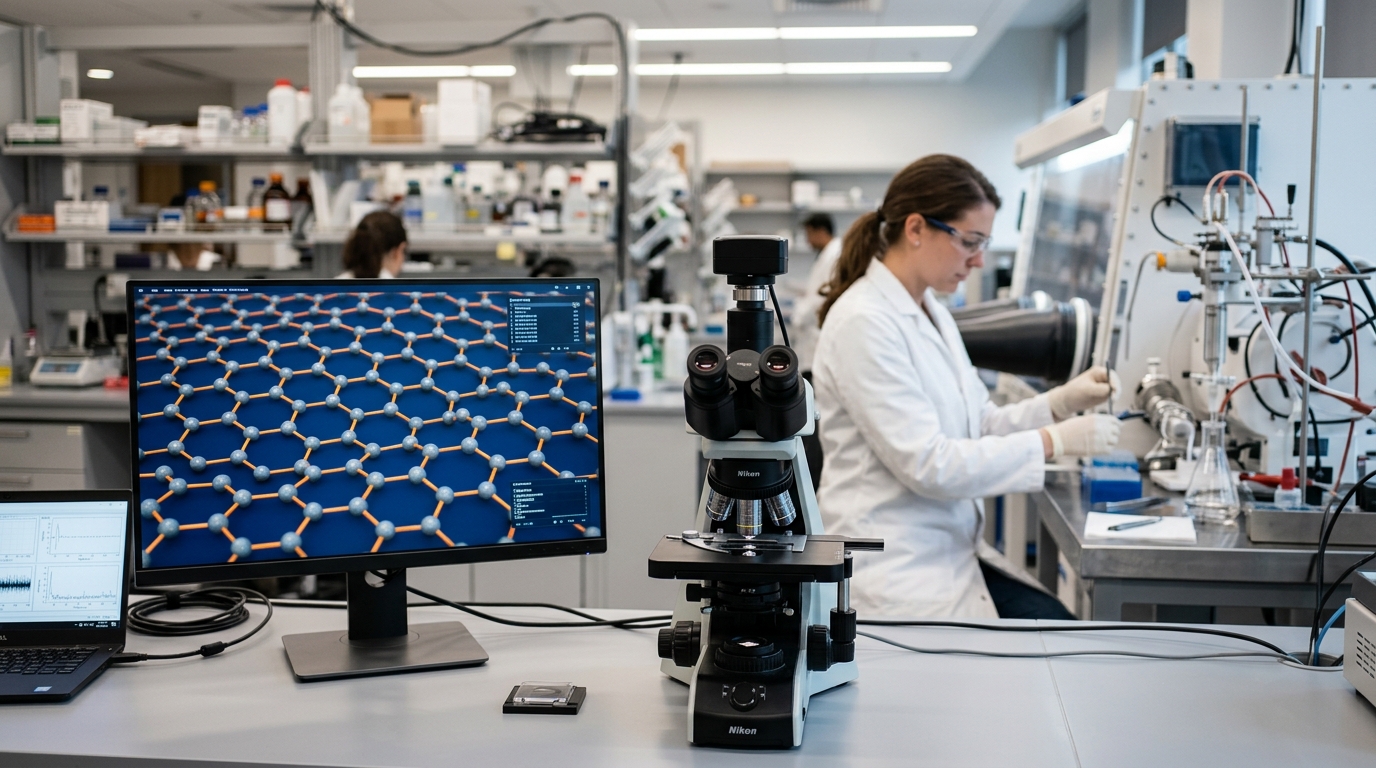
Adisyn said on April 20, 2026, that it had demonstrated a continuous graphene layer on a 1-centimeter coupon using an industrial atomic layer deposition system, a result the company says brings the material closer to semiconductor manufacturing than earlier lab-scale work. The process ran well below 450C, a temperature threshold that matters in chip fabrication because advanced interconnect materials must fit within tightly constrained thermal budgets.
Graphene formed on an industrial ALD system
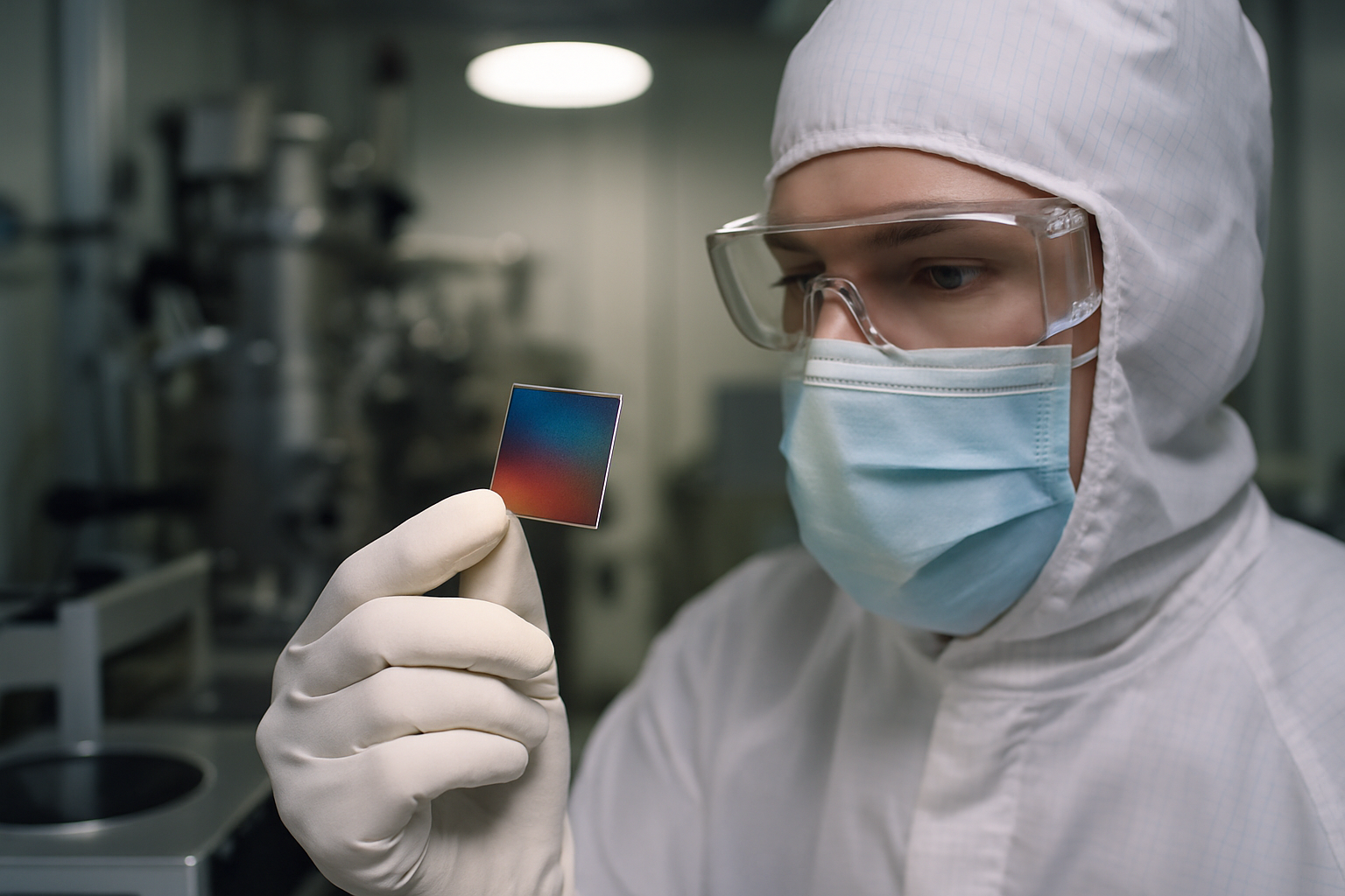
The company said the film was produced on standard industrial equipment rather than through a transfer-based laboratory method. That distinction is central to the announcement: semiconductor manufacturers are unlikely to adopt a material that requires entirely new tooling or a disruptive process redesign. Adisyn said the demonstration showed full graphene coverage on the coupon and used characterization tests to confirm the film’s continuity.
In practical terms, the result is an early proof point for a manufacturing route that could be compatible with existing fabrication lines. The company said the next phase will focus on optimization, repeatability testing and movement toward wafer-level formats, which are the steps that typically determine whether a materials breakthrough can leave the lab.
Why the interconnect problem matters now
Adisyn is targeting copper interconnects, the wiring layers that link billions of transistors in advanced chips. As device geometries continue to shrink, copper faces higher resistance, more heat and greater power loss, all of which pressure performance and energy efficiency. The company is positioning graphene as a possible alternative because of its electrical and thermal properties, especially for high-performance computing, AI, GPU, CPU and networking chips.
The technical challenge has not been graphene itself, but how to form it under semiconductor constraints. Adisyn said its process stays within the industry’s thermal limits and could therefore support a post-copper interconnect approach if the material can be optimized and scaled reliably.
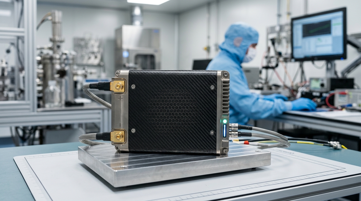
From coupon-scale proof to commercial engagement
The company said the demonstration allows it to move into industry collaboration and commercial engagement, including discussions with Tier 1 semiconductor companies. That is still far from product deployment, but it is the first stage in a commercialization path that depends on repeatable film quality, scalable wafer processing and integration with existing chip production standards.
For the graphene sector, the update is notable because it shifts attention from bulk materials and energy products toward one of the most demanding industrial markets. If the process can be reproduced consistently at scale, the commercial relevance would extend beyond graphene as a research material and toward a manufacturing input for next-generation semiconductors.
Source: Adisyn Ltd ASX Announcement
Date: 2026-04-20