Understanding Graphene Field-Effect Transistors: Mechanics and Potential
Graphene-based field-effect transistors (GFETs) represent a significant area of investigation within the field of electronics and sensor development. By leveraging the unique electrical properties of a single layer of carbon atoms, these devices aim to create components that are thinner, faster, and more sensitive than those currently manufactured using traditional silicon-based architectures.
While silicon has been the backbone of the electronics industry for decades, its physical limitations are becoming more apparent as devices shrink. GFETs offer a potential alternative, particularly in applications requiring extreme sensitivity to environmental changes or high-speed data processing. Understanding their current role requires separating the proven laboratory capabilities from the challenges of mass-market manufacturing.
Quick Summary
| Feature | Details |
|---|---|
| Main Use | High-frequency sensing and signal transduction |
| Material Type | Atomically thin carbon allotrope |
| Development Stage | Applied research and prototype testing |
| Key Advantage | High carrier mobility and surface sensitivity |
| Main Challenge | Lack of a natural bandgap for switching |
| Best-Fit Industries | Biomedical diagnostics, environmental monitoring |
How the Technology Works
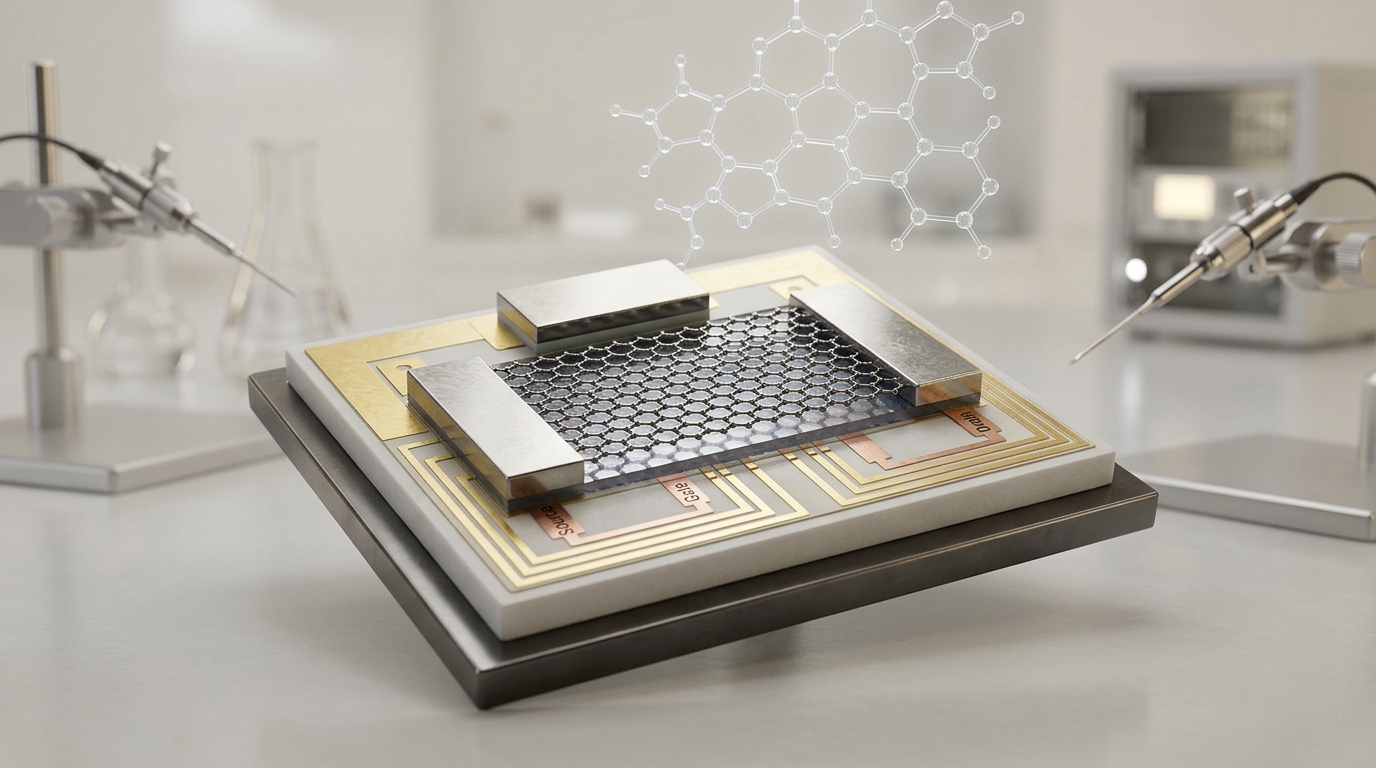
At its core, a GFET functions similarly to a standard transistor, using an electric field to control the flow of electrical current through a channel. In a GFET, the channel consists of a graphene sheet. Because graphene is a semimetal with high charge-carrier mobility, electrons can move through it with minimal resistance, which is the foundational principle for its theoretical speed advantage.
The primary mechanism of action for sensing is the surface-sensitive nature of the material. Because every atom in graphene is exposed to the environment, the electrical conductance of the channel changes instantly when molecules bind to its surface. This sensitivity allows the device to act as a highly effective transducer, converting chemical or biological interactions into measurable electrical signals.
Real-World Applications
- Biosensing: Detecting specific proteins or DNA markers in medical diagnostic platforms.
- Gas Sensing: Monitoring air quality by identifying trace levels of environmental pollutants.
- High-Frequency Electronics: Exploring potential for faster signal processing in specialized communication equipment.
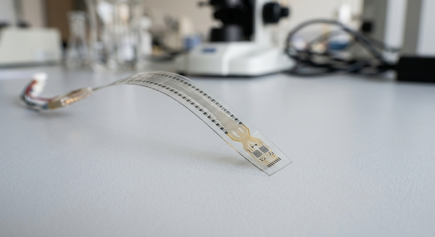
- Wearable Health Monitors: Integrating sensors into flexible substrates to track physiological data in real-time.
Benefits and Limitations
| Factor | Opportunity | Limitation |
|---|---|---|
| Conductivity | High electron mobility | Zero bandgap makes “off” state difficult |
| Sensitivity | Extreme surface-to-volume ratio | Susceptible to environmental noise |
| Scalability | Potential for thin-film integration | High-quality large-area synthesis is costly |
Commercial Readiness
GFET technology is currently transitioning from basic research to specialized commercial application. While you will not find graphene transistors replacing silicon in consumer CPUs, they are appearing in high-end lab-on-a-chip diagnostic tools and specialized environmental sensors. The primary barrier remains the difficulty of manufacturing large-area, defect-free graphene consistently at scale.
Market and Industry Outlook
The industry is focused on integrating GFETs into niche markets where their unique sensing capabilities offer a distinct performance edge over traditional materials. Investment is largely directed toward biosensing and medical device companies that can justify the higher cost of these materials through the improved diagnostic accuracy and speed they provide.
Research Insights
Current academic research is heavily focused on bandgap engineering. By modifying the graphene structure—such as creating graphene nanoribbons or stacking layers—researchers are attempting to create an “off” state, which is required for digital logic applications. Progress in this area is steady, but it remains a significant hurdle for general-purpose computing.
Frequently Asked Questions
Can graphene replace silicon in all transistors?
Currently, no. Graphene lacks a natural bandgap, making it difficult to fully switch off, which is a requirement for standard digital logic. It is better suited for specialized sensors rather than general computing.
Why are GFETs considered so sensitive?
Because graphene is only one atom thick, every atom in the channel is a surface atom. This allows any molecule binding to the surface to directly influence the electrical conductivity of the entire device.
Are graphene sensors ready for consumer use?
Some niche sensors are entering the commercial market, but they are generally limited to specific industrial or laboratory settings rather than everyday consumer electronics.
Editorial Disclaimer
This article is provided for educational and informational purposes only. Graphene research and commercialization claims can change quickly, so readers should verify technical specifications with manufacturers, research institutions, or regulatory sources before making business or investment decisions.