UCSB models a single-electron failure mode that shortens silicon chip lifetimes
Researchers at the University of California, Santa Barbara say they have identified the quantum mechanism behind a major reliability problem in microelectronics, tracing a long-studied form of silicon damage to a single energetic electron. The finding, published on April 14, 2026, in Physical Review B, gives materials scientists and chip engineers a more precise way to think about transistor wear as devices shrink and run hotter for longer.
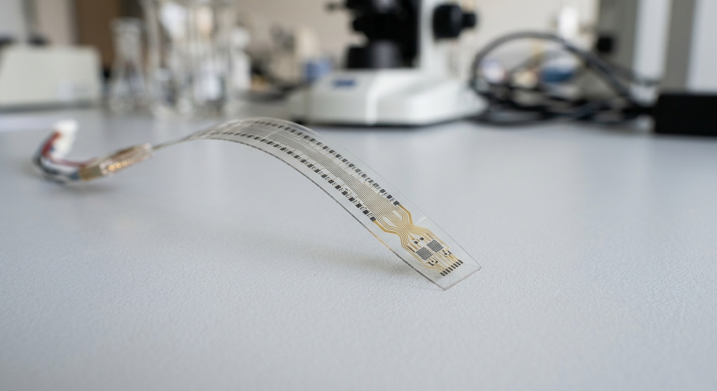
UCSB’s silicon-hydrogen interface model
The team focused on silicon-hydrogen bonds near the silicon-oxide interface inside transistors, where hydrogen is used during manufacturing to neutralize defects. According to the researchers, a high-energy electron can briefly occupy a previously unidentified electronic state, weaken the bond and push hydrogen out of position, exposing a defect that degrades performance.
That mechanism revises the field’s older assumption that the damage builds up only after many electrons strike the same bond. The study says the process is triggered by one electron, not a slow accumulation of impacts, and that hydrogen behaves according to quantum-mechanical rules as it detaches rather than as a classical particle.
Why this matters for chip reliability
Hot-carrier degradation has been one of the persistent limits on how long semiconductor devices keep performing at specification. The UCSB model explains why bond breaking is especially damaging around seven electron-volts, and why the effect is temperature independent. It also accounts for the much slower degradation seen when deuterium replaces hydrogen, a detail that had puzzled experimenters for years.
For the semiconductor industry, that kind of mechanistic clarity matters because reliability failures are not just a lab curiosity. They affect the lifetime of smartphones, laptops, solar cells and medical implants, all of which depend on stable materials at interfaces that are difficult to observe directly in operation.
What the result could change in materials engineering
The broader value of the work is not only explanatory. By turning a hard-to-model failure mode into a predictive framework, the study gives researchers a way to screen which chemical bonds are most vulnerable under electrical stress. That could help guide interface design in silicon and in other semiconductor materials where electron-induced bond breaking limits durability.
The researchers say the same physics may matter in light-emitting diodes and power electronics, including ultraviolet LEDs that face commercialization pressure for disinfection and water-purification uses. In those systems, device degradation can become a manufacturing and deployment problem long before the underlying material reaches its theoretical limits.
A cleaner picture of failure at the nanoscale
The practical significance of the result lies in its specificity. Rather than treating microelectronic wear as a vague materials aging problem, the new model identifies a concrete bond-breaking pathway at a critical interface in the transistor stack. That kind of detail is what materials science often needs before reliability can be engineered rather than merely observed.
For now, the study gives the semiconductor world a more exact target: the atomic-scale interaction between energetic electrons, silicon-hydrogen bonds and the oxide interface that sits at the heart of modern chips.
Source: UC Santa Barbara Engineering
Date: 2026-04-14