Nature study pushes metalenses toward industrial production with 300-per-second roll-to-roll output
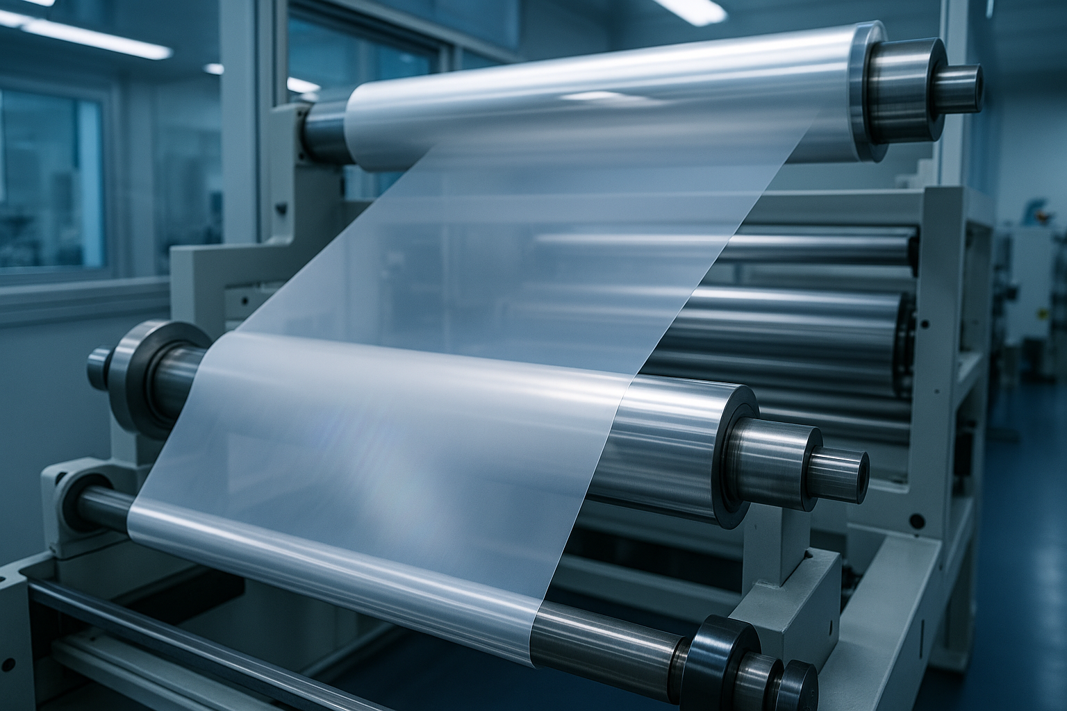
A new Nature study published on April 15, 2026 reports a manufacturing advance that could help move visible metalenses from experimental devices into higher-volume production. The team says it has built an automated roll-to-roll nanoimprinting system capable of producing 300 metalenses per second, with a conformal titanium dioxide coating step used to improve optical performance.
Roll-to-roll nanoimprinting reaches industrial throughput
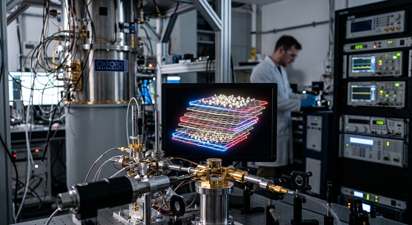
The work centers on visible metalenses, flat optical components built from subwavelength structures rather than curved glass. According to the paper, the process combines continuous roll-to-roll nanoimprinting with atomic layer deposition, allowing the team to fabricate the devices at scale while maintaining uniformity across the patterned area.
That throughput figure matters because metasurface optics have often been compelling in the lab but difficult to manufacture at rates and costs that match commercial requirements. The study says the output cost is comparable with, and in some cases lower than, conventional refractive optics.
Titanium dioxide coating is doing more than fine-tuning the lens
The titanium dioxide layer is not a cosmetic add-on. In the reported process, it serves as a conformal high-index coating that improves the optical behavior of the patterned structures after imprinting. The paper says experimental characterization showed high efficiency, uniformity, and consistent yields across the full patterned area.
That is the practical hurdle for flat optics: not just demonstrating a working device, but proving that the device can be reproduced reliably as a manufacturing object. The study is aimed at that gap, showing a route that pairs nanoscale patterning with a coating step familiar to semiconductor and advanced materials production.
Why the result matters for photonics and manufacturing
If the process holds up beyond the first demonstration run, it could narrow one of the biggest barriers to commercial metasurfaces: production speed. Metalenses have long been pitched for compact imaging, sensing, and other photonics applications, but scale has been the missing piece.
The reported system suggests a path toward lower-cost flat optics that can be made continuously rather than one wafer or one prototype at a time. That does not mean mass-market deployment is immediate, but it does place the technology closer to the kind of repeatable process engineering investors, device makers, and production teams look for before committing to volume adoption.
A commercialization signal, not just a laboratory result
The most important detail in the paper is not that metalenses can work; it is that they can be made continuously at a rate that starts to resemble industrial output. In materials science, that is often the difference between an elegant publication and a platform that can be engineered into products.
For optics makers and manufacturers weighing flat-lens adoption, the question now shifts from whether the devices can function to how quickly the process can be transferred, qualified, and integrated into real production lines.
Source: Nature
Date: 2026-04-15