Nature Materials spotlights ultrathin van der Waals hard masks for 3D chip etching
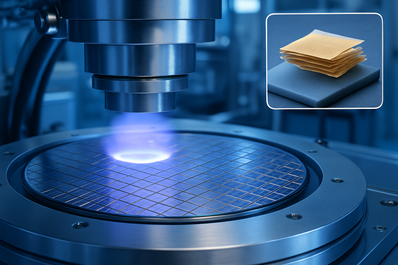
Nature Materials on April 16, 2026 highlighted a class of ultrathin van der Waals metal oxyhalides that can act as hard masks for three-dimensional semiconductor processing. The materials are described as unusually resistant to plasma, with a smoothing effect that helps support more precise nanopatterning at advanced device scales.
Van der Waals metal oxyhalides move into chip-patterning workflows
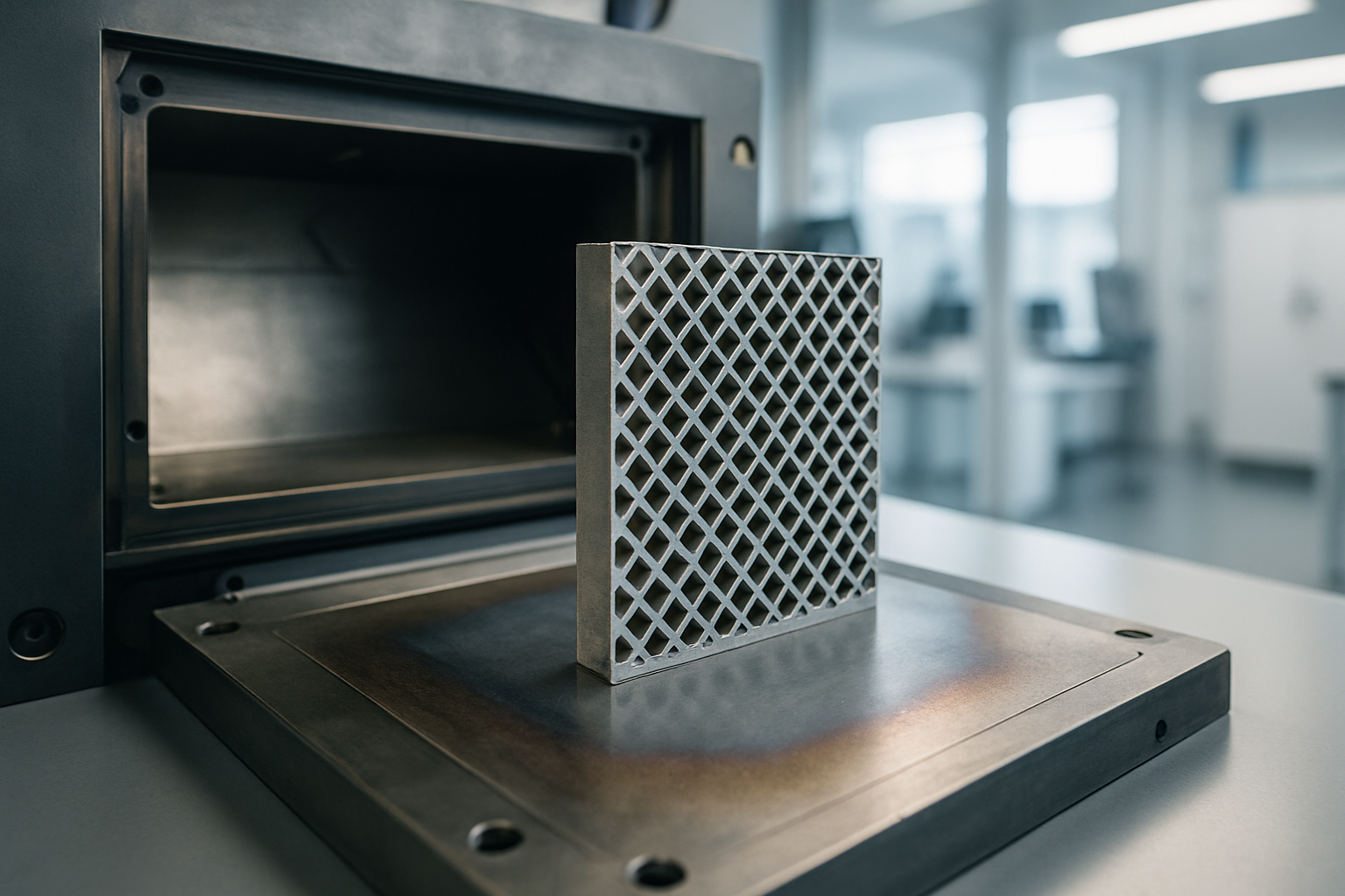
The report centers on using atomically thin metal oxyhalides as hard masks in etching steps that shape increasingly complex semiconductor structures. In practical terms, that points to a route for pattern transfer that is thinner than many conventional masking materials, yet still durable enough to survive aggressive plasma conditions.
The appeal is operational as much as scientific. As chipmakers push toward denser, more three-dimensional architectures, the mask itself becomes a critical part of the patterning stack. Materials that remain intact under etch exposure while preserving fine features can help reduce pattern distortion and improve feature fidelity.
Why plasma resistance matters for high-aspect-ratio structures
According to the Nature Materials summary, the key advantage is the combination of plasma resistance and plasma-induced smoothing. Those properties are especially relevant in high-aspect-ratio etching, where small defects or rough edges can be amplified as features are etched deeper into a substrate.
That makes the development relevant beyond a single materials class. If the approach scales, it could improve the reliability of nanopatterning across a range of materials and device designs, from advanced logic to other nanoscale platforms that depend on sharp, repeatable pattern transfer.
Where the development stands now
The Nature Materials item is a News & Views entry rather than a commercial product announcement, so it should be read as an indicator of technical momentum rather than an industrial rollout. Even so, its timing is notable: the field continues to look for mask materials that can keep pace with tighter geometries without sacrificing process stability.
For nanomaterials research, the significance is straightforward. The work points to a materials-engineering answer to a manufacturing problem, with ultrathin van der Waals compounds being evaluated not just for their structure, but for how they behave under the harsh conditions of semiconductor fabrication.
Source: Nature Materials
Date: 2026-04-16