Graphene-sealed imaging opens a new route to studying air-sensitive 2D materials
Researchers at the University of Manchester say they have captured the first atomic-resolution images of monolayer transition metal diiodides, using graphene encapsulation to keep the materials from degrading the moment they meet air. The advance is notable not because it introduces a new 2D compound, but because it solves one of the field’s most stubborn practical problems: how to study highly reactive atomically thin crystals before they fall apart.
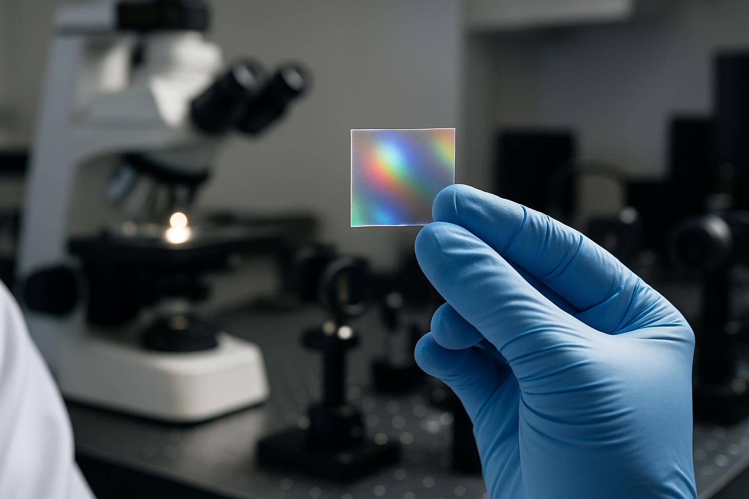
Graphene encapsulation preserves a material that usually vanishes in seconds
The team’s samples were built around a graphene-sealed transmission electron microscopy preparation method that prevents rapid degradation and preserves atomically clean interfaces. According to the researchers, the approach extends the usable lifetime of these monolayers from seconds to months, creating a window long enough for both structural analysis and transport between facilities.
That durability matters because transition metal dihalides have long been considered promising for electronics, photonics, and quantum devices, but their extreme reactivity has made even basic characterization difficult. In this case, the encapsulation was not a cosmetic packaging step; it was the enabling technology that made the imaging possible at all.
Atomic images expose defects and edge evolution in monolayer diiodides
With stable samples in hand, the researchers were able to observe local structural variations in the thinnest crystals, along with atomic defect dynamics and changes at the material edge. Those details matter in 2D materials because atomic-scale disorder often determines whether a crystal behaves as a useful device layer or as an academic curiosity.
The work also suggests that the same sealing strategy could help researchers move from speculation to measurement on other reactive 2D compounds that have resisted ordinary fabrication and microscopy workflows. For a field built on manipulating matter one layer at a time, the bottleneck is increasingly not discovery alone but sample survival.
Why the result matters for the next wave of 2D devices
The immediate significance is operational: if a material can be sealed cleanly enough to survive air exposure, it can be studied, compared, and transferred with far less loss of information. That improves the odds that predicted properties in reactive 2D materials can be checked against real devices rather than inferred from incomplete samples.
It also gives labs a more realistic path to reproducible measurements on compounds that were previously too fragile to handle outside tightly controlled conditions. The broader result is a reminder that in two-dimensional materials research, progress increasingly depends on interface control and packaging as much as on the crystals themselves.
Source: Phys.org / University of Manchester
Date: 2026-02-04