What Is Graphene Rippling? A Practical Guide to the Material’s Hidden Waviness
Graphene rippling is the formation of tiny waves, wrinkles, and corrugations in a graphene sheet. Because graphene is only one atom thick, it does not stay perfectly flat in the way a sheet of paper does. Its atoms can bend, buckle, or undulate at very small scales, and those shape changes can influence electrical behavior, heat flow, mechanical response, and how the material attaches to surfaces.
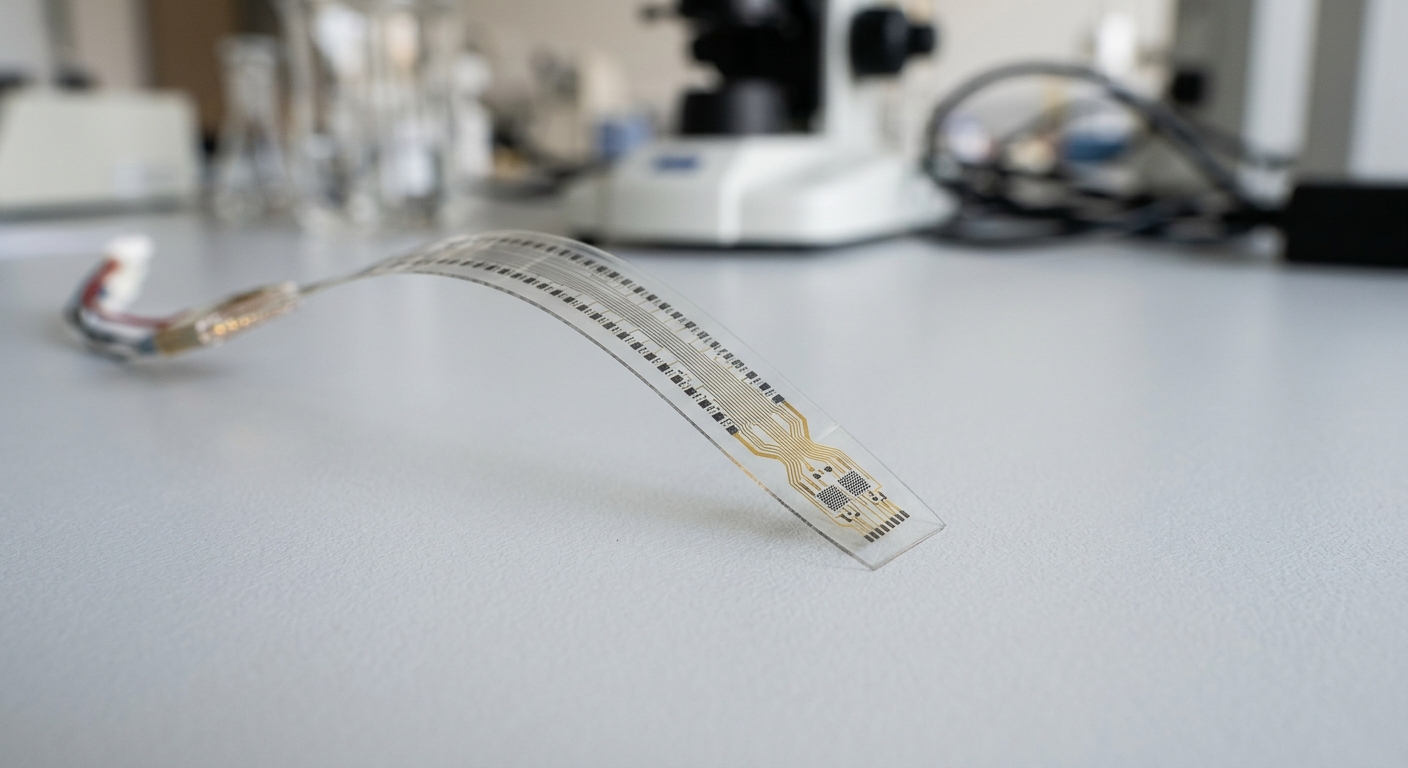
That matters because most graphene products are not used as isolated, idealized sheets. They are built into coatings, electrodes, films, composites, sensors, and other real-world structures where the sheet must interact with solvents, substrates, polymers, or metal surfaces. In those settings, rippling can be either a nuisance or a useful feature, depending on the application.
Graphene rippling is the sheet’s natural nanoscale waviness
In plain terms, rippling means the graphene lattice is no longer perfectly flat. The distortion may appear as gentle out-of-plane waves, localized wrinkles, or more complex corrugated patterns. The geometry can arise during growth, transfer, drying, stretching, or cooling, and it may persist after the graphene is placed into a device or composite.
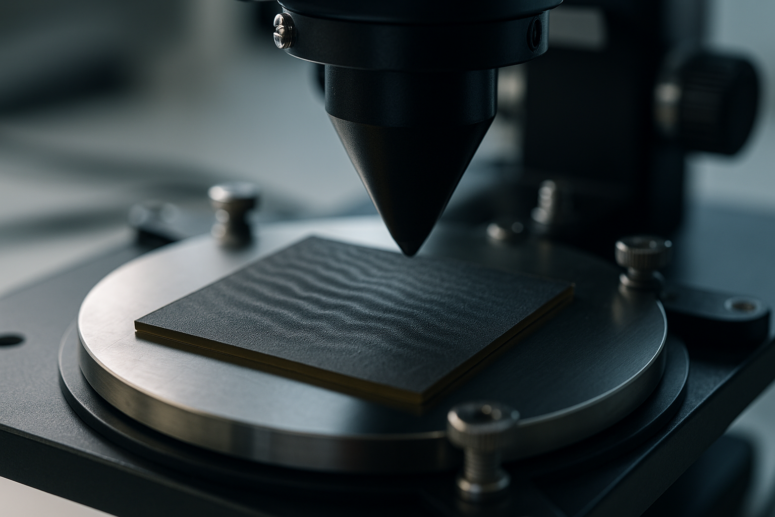
Because graphene is so thin, even small disturbances can change its shape. A substrate beneath it may not be perfectly smooth. Thermal mismatch between graphene and a supporting layer can create stress. Adsorbed molecules, contamination, grain boundaries, and edge constraints can all contribute. The result is a material that often looks flat at ordinary scale but is highly textured under nanoscale inspection.
Why manufacturers care about rippling in coatings, sensors, and electronics
Rippling affects performance because graphene’s electronic and mechanical properties depend not only on its chemistry but also on its geometry. A flat, continuous sheet can behave differently from a rippled one when current moves across it, when heat spreads through it, or when it is asked to sense pressure, strain, gas molecules, or biomolecules.
For sensor designers, some amount of corrugation may help increase active surface area or create more interaction sites. For electronics, however, uncontrolled rippling can raise variability and make device behavior harder to reproduce. In coatings and composites, wrinkles can change how well graphene disperses, how it bonds with the host material, and whether it forms a reliable conductive network.
That tradeoff is one reason graphene has been easier to demonstrate in laboratories than to standardize across industrial production. A nanoscale effect that is acceptable in one product can be a defect in another.
What causes graphene to ripple during production and transfer
Several manufacturing steps can introduce ripple formation. During growth, especially when graphene is made on a metal surface, the film may inherit stress from the underlying template. When it is removed and transferred to another substrate, the release process can leave behind strain, folding, or uneven adhesion. Drying after wet processing can also pull the sheet into new shapes as liquids evaporate and surface tension acts across the film.
Temperature changes are another major factor. Graphene expands and contracts differently from many substrates, so heating and cooling cycles can create compressive or tensile stress. In multilayer stacks, trapped residues or uneven interfaces can produce local buckling. Even when a process starts with a high-quality sheet, the final device may contain a network of ripples created during integration rather than during synthesis itself.
How ripples change graphene’s behavior in real devices
The practical effects depend on the size, spacing, and regularity of the ripples. Gentle, controlled corrugation may be useful if a product needs flexibility, strain tolerance, or extra surface area. Irregular wrinkles can be harder to manage because they may scatter charge carriers, create local strain fields, or introduce unpredictable contact resistance.
In thermal management applications, a rippled sheet may not spread heat as efficiently as a smoother one if the distortions interrupt in-plane transport or reduce contact with the substrate. In conductive coatings and printed electronics, the issue may be continuity: a network that looks complete under a microscope can still have weak points if ripples interfere with percolation or adhesion.
For chemical and biological sensors, the effect is more nuanced. Rippling can expose more active area and sometimes improve sensitivity, but it can also complicate calibration. A sensor that changes behavior with strain, humidity, or repeated handling may be harder to deploy outside the lab.
The manufacturing challenge is control, not just observation
The main industrial question is not whether graphene ripples exist. They do. The question is whether producers can control when they appear, how large they are, and whether they improve or degrade the final product. That requires better control over growth conditions, transfer chemistry, substrate preparation, and post-processing.
It also requires measurement. Companies and research labs need to know whether a ripple pattern is uniform enough for a coating, benign enough for a composite, or damaging enough for an electronic layer. That often means combining microscopy with electrical, mechanical, and thermal testing rather than relying on a single inspection method.
For commercialization, this is one of graphene’s quiet but important scale-up issues. A material can look promising at the wafer or flake level and still prove difficult to make reproducibly when the process moves to pilot lines and large-area films.
Graphene rippling is therefore best understood as a structural feature with practical consequences: sometimes useful, sometimes unwanted, and always tied to how the material is made and used. For researchers and product developers, the real task is to turn that waviness from an uncontrolled side effect into something measurable, predictable, and fit for purpose.