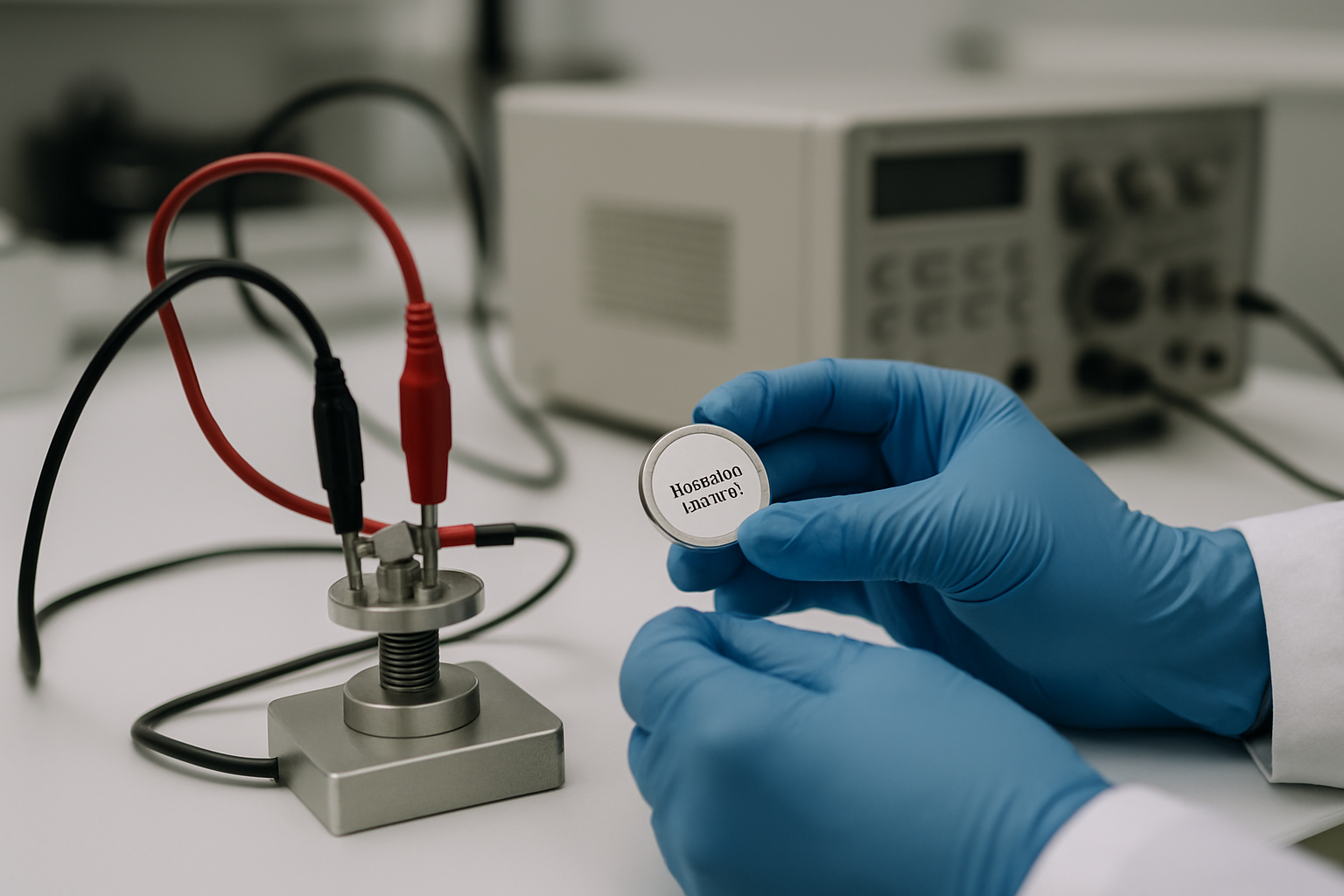
Black Semiconductor wins €211 million to build graphene photonics pilot line in Aachen
Black Semiconductor has secured €211 million in public support for its graphene photonics program in Aachen, giving one of Europe’s most closely watched graphene-chip efforts a clearer route from lab work to pilot manufacturing. The company said the funding will help it move toward a 300-millimeter wafer pilot line for integrated graphene photonics, a process intended to link electronic and optical functions on the same chip platform.
Aachen project gets the money to leave the lab
The new financing is newsworthy because it is tied to manufacturing, not just research. Black Semiconductor’s goal is to build a pilot line large enough to work at semiconductor-industry scale, using 300-mm wafers rather than the smaller substrates common in early-stage materials development. That shift matters because it is one of the few ways graphene-based chip concepts can be evaluated under conditions that resemble real production.
The company’s approach centers on integrated graphene photonics, which aims to use graphene in chip architectures where electrical signaling and optical communication can be combined. In practical terms, that could help address bandwidth and energy bottlenecks inside advanced computing systems, where short-range interconnects are increasingly a limiting factor.
Why a 300-mm line changes the commercial picture
Graphene has long attracted semiconductor interest because of its electrical and thermal properties, but commercial progress has been slowed by scale-up, uniformity and compatibility problems. A 300-mm pilot line does not solve those issues by itself, but it gives engineers a production environment to test whether graphene materials and processes can survive the requirements of volume fabrication, process control and device integration.
For the chip industry, that is the meaningful threshold. If Black Semiconductor can prove reproducibility on large wafers, the technology becomes easier to compare with existing interconnect and photonics options on cost, yield and integration risk, rather than on laboratory performance alone.
What the funding means now
The funding also gives the Aachen project a more concrete timeline than most graphene semiconductor announcements. Instead of a distant promise of post-silicon logic, the focus is on pilot manufacturing, materials integration and process development. That makes the project relevant not only to semiconductor researchers, but also to equipment suppliers, materials companies and chipmakers looking for ways to reduce data-transfer losses inside advanced systems.
Even with the new support, the work remains early-stage. Graphene photonics still has to prove it can be manufactured reliably at scale, but the latest commitment moves the field one step closer to an industrial test case rather than a research program.
Source: Black Semiconductor
Date: 2026-04-20