Paragraf’s 6-inch graphene wafer push sharpens the race to commercial sensors
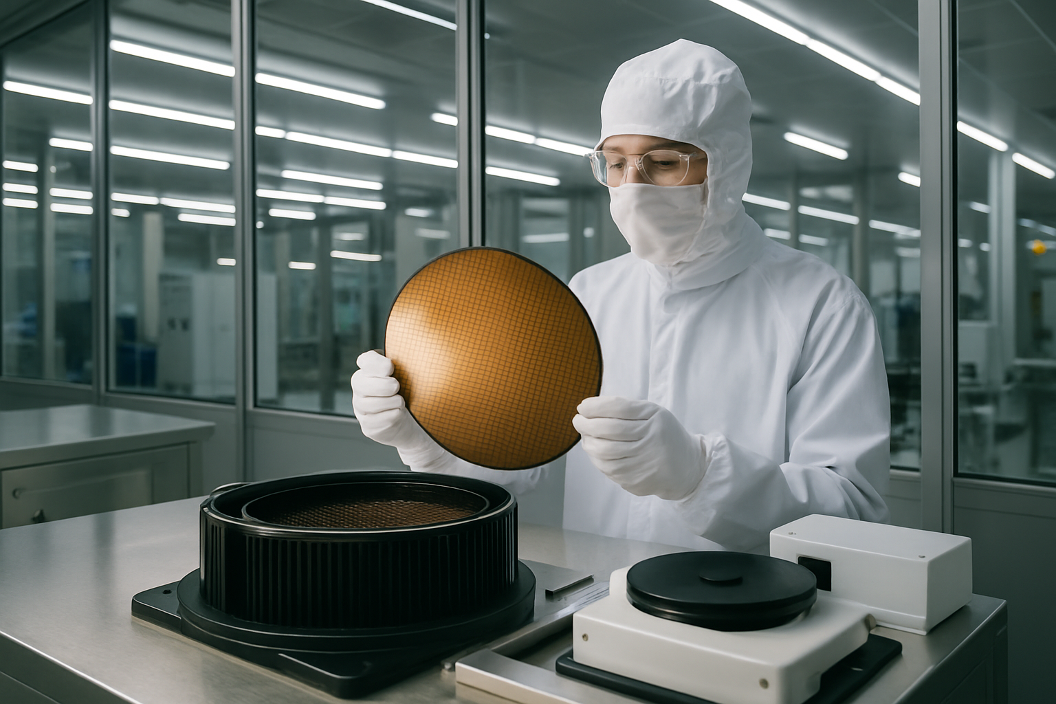
Paragraf says it has produced its first 6-inch graphene wafer at a new manufacturing facility in Huntingdon, England, a step that advances one of the clearest commercial efforts in graphene electronics and sensors. The company framed the wafer as a production milestone for its transfer-free graphene platform, which is aimed at semiconductor-style manufacturing rather than laboratory-scale fabrication.
First 6-inch wafer marks a scaling step
The announcement centers on the company’s ability to manufacture a larger graphene wafer at its new site, a change that matters because sensor developers typically need consistent wafer-scale output before they can move from prototypes to repeatable production. Paragraf said the wafer was produced at the Huntingdon facility, expanding the company’s manufacturing capability and technology platform.
For graphene sensors, the practical significance is less about the material itself than about process control. Wafer size, uniformity and compatibility with standard semiconductor workflows are all critical if the technology is going to move beyond bespoke devices and into higher-volume sensor manufacturing.
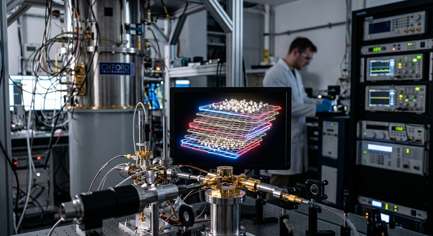
Why wafer-scale graphene matters for sensors
Graphene-based sensors have been promoted for applications ranging from magnetic and chemical sensing to biosensing, but scale-up has remained a central hurdle across the field. A larger wafer format can make it easier to integrate devices into established production lines, simplify packaging and testing, and support more consistent performance from batch to batch.
That is especially relevant for industrial and diagnostic markets, where buyers generally want reliability, supply continuity and a clear path to volume production before they commit to a new sensing platform.
Paragraf’s commercialization pitch
Paragraf has positioned itself as a manufacturer of graphene electronics using standard semiconductor processes, and the company has been building out a sensor portfolio around graphene field-effect transistors and related devices. The new wafer result suggests the company is still focused on turning that platform into a manufacturing business, not just a research program.
The company did not disclose in the announcement any customer shipment tied to the wafer milestone, and the immediate significance lies instead in production readiness. In a sector where many graphene sensor efforts remain stuck at proof-of-concept stage, the move to a 6-inch wafer is a concrete indicator of scale-up progress.
What the Huntingdon result signals next
The broader market for graphene sensors still depends on whether manufacturers can deliver repeatability, yield and cost control at levels that make commercial deployment practical. Paragraf’s latest step does not resolve those questions, but it does move the company further toward the kind of process maturity that sensor customers usually want to see before volume adoption.
For now, the key development is that graphene sensor manufacturing has moved another notch closer to standard semiconductor production, with the first 6-inch wafer now coming out of the new Huntingdon facility.
Source: Paragraf
Date: 2026-01-15