Rice team says symmetry boost pushes 2D perovskites past 2-micrometer exciton travel mark
Rice University researchers and collaborators have reported a new two-dimensional perovskite that keeps its crystal structure unusually symmetrical at room temperature, enabling excitons to move more than 2 micrometers without losing energy. The result, published April 2, 2026 in Nature Synthesis, is a notable step for a material family closely watched for solar cells, photodetectors and other optoelectronic devices.
Rice pins a sharper crystal structure on multilayer 2D perovskites
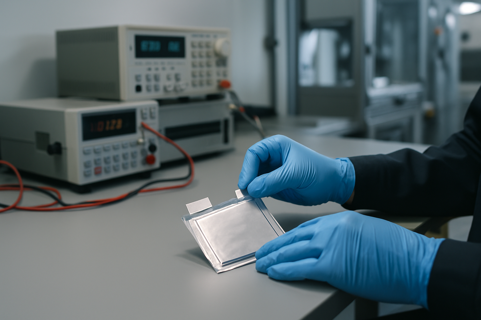
The team said it engineered a multilayer 2D metal halide perovskite that avoids the structural distortions that typically limit performance in softer perovskite lattices. In the researchers’ description, the material is the first demonstrated multilayered 2D perovskite system at room temperature to reach what they call maximum symmetry, with excitons traveling more than 2 micrometers.
That transport distance is the headline technical gain. The study says the new material’s exciton diffusion performance is an order of magnitude better than previously reported perovskites and comparable to monolayer transition metal dichalcogenides, a separate class of 2D materials already used in sensors and integrated electronics.
Why the 2-micrometer exciton path matters for devices
In optoelectronics, losing too much energy as light is absorbed and converted can quickly limit efficiency. Longer exciton diffusion gives device designers more room to separate charges before they recombine, which can help with photodetectors, solar cells and layered tandem architectures that depend on efficient light capture across different parts of the spectrum.
Rice said proof-of-concept self-powered photodetectors built from the new material were more sensitive and responded faster than devices made from a different 2D perovskite, especially in thicker films. The work also points to tandem solar-cell use, where the material’s band gap may better complement silicon or other perovskites.
A temperature-tuned fabrication route kept the lattice intact
The group said the advance depended on a different manufacturing approach: rather than letting crystals form as a solution cooled, it removed them at higher temperatures to lock in the desired structure before it could transform. That also let the researchers produce thicker multilayer forms, rather than the thinner versions that had limited earlier attempts.
One co-author said the new configuration connects three or more perovskite layers, expanding on prior work that had only managed two. The paper also notes that the researchers have filed a patent on the fabrication method, a sign that the result is being positioned with an eye toward repeatable processing rather than only laboratory demonstration.
Where the 2D materials race is headed next
For the broader 2D materials field, the result lands in a moment when researchers are pushing beyond graphene toward materials with more tunable electronic and optical behavior. Here, the practical value is not just in the symmetry claim itself, but in the combination of structural control, room-temperature stability and device-level testing in the same study.
If the fabrication route scales cleanly, the material could become a candidate for layered optoelectronics where stability and charge transport both matter. For now, the most concrete milestone is the reported diffusion length: more than 2 micrometers in a room-temperature multilayer 2D perovskite, with device tests already showing faster and more sensitive response.
Source: EurekAlert! / Rice University
Date: 2026-04-03