Laser-Tuned Graphene Opens a New Route for Precision Thin-Film Manufacturing
Researchers in Finland say they have found a way to use laser-modified graphene to control where ultra-thin films grow, a development that could improve the precision of advanced materials manufacturing.
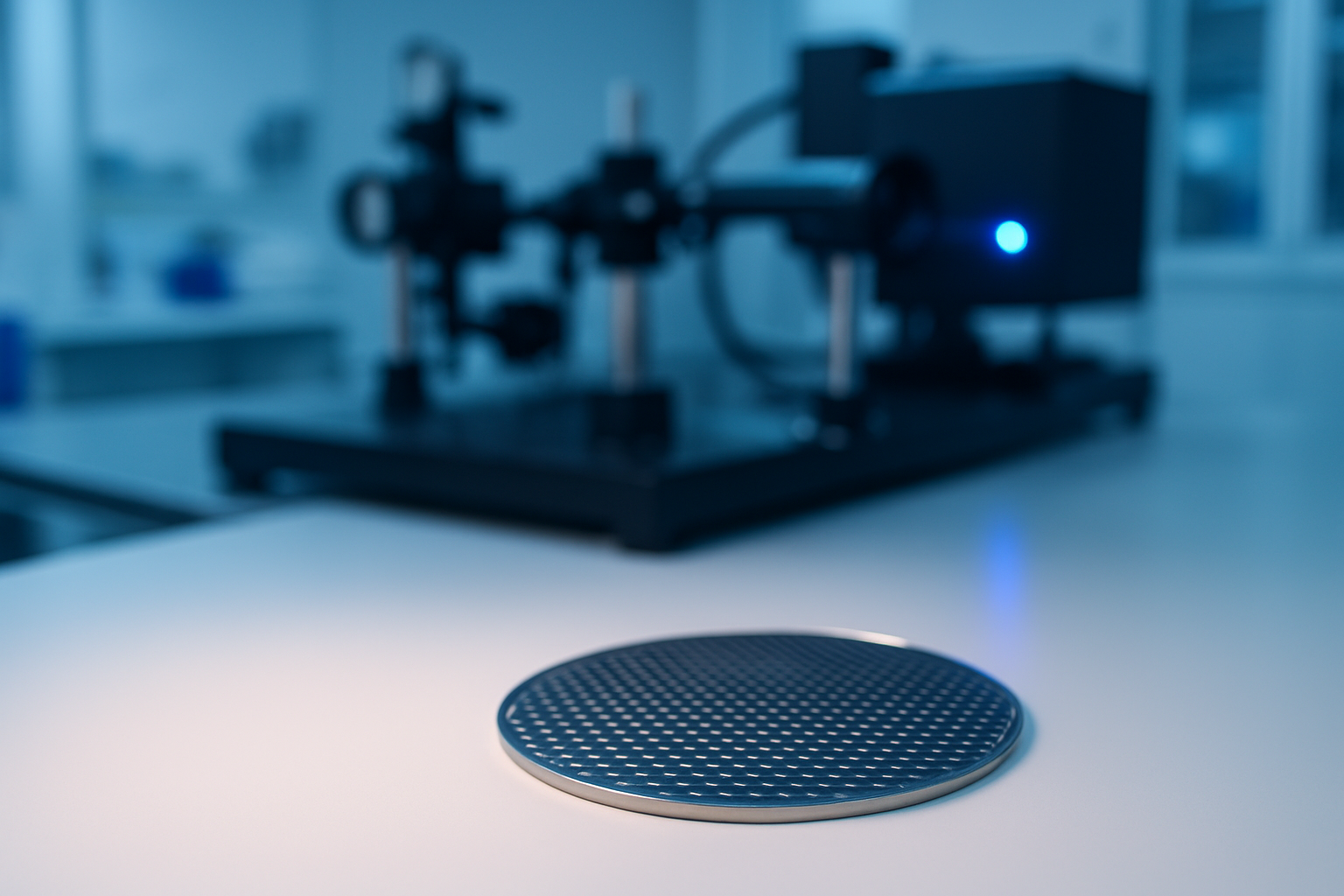
The work, reported on March 25, 2026, and published in ACS Nano, describes an area-selective deposition method in which graphene is first prepared on a silicon chip and then modified with laser light in specific places. Those laser-treated regions can attract a europium organic thin film, while untreated graphene does not react in the same way.
What the researchers reported
In the study, teams from the University of Jyväskylä and Aalto University said the method enables one-molecule-thick films to be grown only where needed. That kind of control is important for building materials with carefully engineered properties.
The researchers said the approach could open the door to a wider range of thin-film materials, not just the europium-based model system used in the study. They also suggested the technique could be relevant for future applications in electronics, optics and other device platforms.
Why graphene matters here
Graphene served as the base surface for the experiment because of its role as an atom-thin carbon film with highly tunable surface behavior after laser treatment. By changing only selected areas, the scientists were able to make the graphene surface chemically active in a controlled way.
That selective reactivity is what allowed the material to guide deposition with greater spatial precision. In practical terms, the method could help manufacturers build small, complex structures without coating an entire surface.
What could come next
The researchers said the next step is to develop applications and explore whether companies may be interested in the method. For now, the result remains a research-stage advance, but it adds to the growing list of graphene-based techniques aimed at making materials processing more exact.
- Scientists used laser-modified graphene to direct thin-film growth in specific areas.
- The work was reported on March 25, 2026, and published in ACS Nano.
- The method could have future uses in advanced electronics and photonic materials.
What to Watch
Watch for follow-up studies that test whether the technique can be scaled beyond laboratory samples and adapted to other materials systems. The key question now is whether the selective-growth method can move from a proof of concept to a tool that manufacturers can use in real device production.
Source Reference
Primary source: Phys.org
Source date: 2026-03-25
Reference: Read original source