Graphene
Graphene is a single layer of carbon atoms arranged in a two-dimensional hexagonal honeycomb lattice. As the fundamental structural element of other carbon allotropes—including graphite, carbon nanotubes, and fullerenes—it represents the thinnest, strongest, and most conductive material ever isolated. While graphite has been used for centuries, isolating an individual atomic plane was long considered thermodynamically impossible at room temperature until researchers successfully isolated monolayer graphene in 2004 using mechanical exfoliation.
Understanding graphene requires moving beyond generic claims of a wonder material to examine its physical chemistry, synthesis methods, material forms, and realistic engineering trade-offs. The properties measured on a pristine, microscale flake in an ultra-high vacuum do not automatically transfer to bulk industrial materials. Evaluating graphene requires matching the appropriate material grade—whether continuous monolayer films, microscopic flakes, or functionalized derivatives—to the specific electrical, mechanical, or thermal performance requirements of a given engineering challenge.
The Physics and Atomic Structure of Two-Dimensional Carbon
Graphene owes its extreme properties to the quantum mechanical behavior of carbon electrons in a planar configuration. Each carbon atom possesses four valence electrons. In the graphene lattice, three of these electrons undergo sp² hybridization, forming robust covalent sigma (σ) bonds with three neighboring carbon atoms. These in-plane bonds have an exceptionally short bond length of approximately 0.142 nanometers, which gives the lattice its extraordinary in-plane mechanical rigidity and tensile strength.
The fourth valence electron occupies an unhybridized p_z orbital oriented perpendicular to the atomic plane. These orbitals overlap across adjacent atoms to generate a delocalized network of pi (π) and pi-star (π*) electron bands. The electronic band structure of graphene is unique: the conduction and valence bands touch at distinct points at the corners of the hexagonal Brillouin zone, known as Dirac cones.
Because the energy-momentum dispersion relation around these points is linear rather than parabolic, charge carriers (electrons and holes) behave as massless relativistic particles described by the Dirac equation rather than the standard Schrödinger equation. This quantum phenomenon allows electrons to travel across micron-scale distances without scattering at room temperature, creating exceptionally high electrical conductivity and room-temperature quantum Hall effects.
The Spectrum of Graphene Materials
In commercial and scientific practice, the term graphene refers to a family of materials rather than a single uniform substance. The International Organization for Standardization (ISO) and materials science conventions classify graphene-related materials based on their layer count, lateral dimensions, carbon-to-oxygen ratio, and production method. Treating these distinct forms interchangeably is the primary source of misconception regarding performance and cost.
| Material Form | Layer Count | Typical Lateral Size | Primary Production Method | Dominant Industrial Uses |
|---|---|---|---|---|
| Monolayer / Bilayer CVD Graphene | 1 to 2 layers | Millimeters to meters (continuous film) | Chemical vapor deposition on catalytic metal foils | High-frequency electronics, transparent conductive electrodes, photonic sensors |
| Graphene Nanoplatelets (GNPs) | 3 to 30+ layers | 0.5 to 50 micrometers | Liquid-phase exfoliation, shear mixing, plasma expansion | Polymer composites, conductive inks, thermal interface materials, lubricants |
| Graphene Oxide (GO) | 1 to few layers (heavily oxygenated) | 0.1 to 20 micrometers | Chemical oxidation and exfoliation of graphite flakes | Water filtration membranes, energy storage slurries, biosensors |
| Reduced Graphene Oxide (rGO) | 1 to few layers (defective lattice) | 0.1 to 20 micrometers | Thermal, chemical, or photochemical reduction of GO | Electrode coatings, electromagnetic shielding, functional coatings |
Monolayer and Few-Layer Graphene
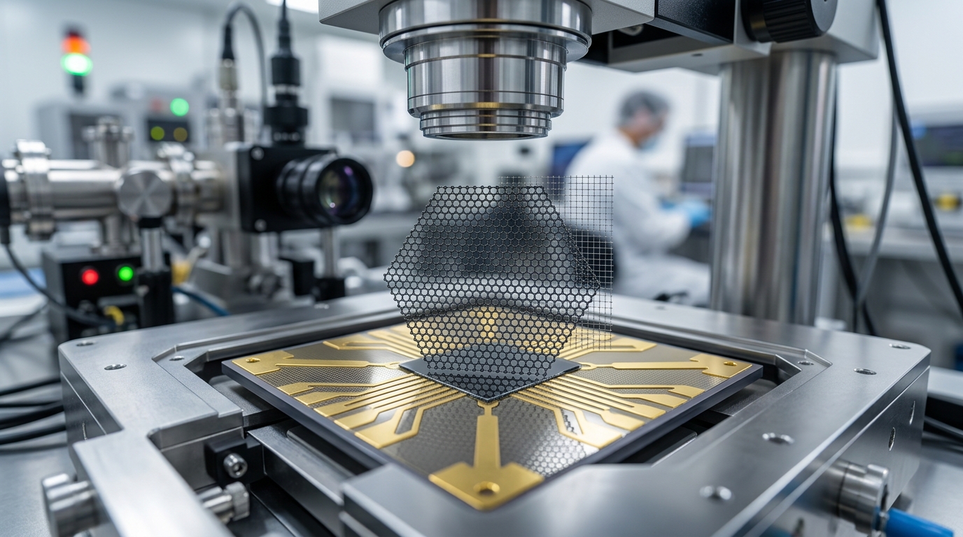
True monolayer graphene consists of a single continuous sheet of carbon atoms. High-purity monolayer material is typically produced via chemical vapor deposition (CVD) onto catalytic substrates such as copper or nickel foils. While CVD graphene delivers near-theoretical electrical mobility and optical transparency, it is expensive to manufacture and delicate to transfer onto non-metallic substrates such as silicon or flexible polymers.
Graphene Nanoplatelets (GNPs)
Graphene nanoplatelets (GNPs) consist of multi-layer stacks ranging from 3 to several dozen atomic layers, typically retaining graphite-like stacking order while preserving high aspect ratios and thin cross-sections. GNPs lack the relativistic Dirac electronic behavior of isolated monolayers, but they provide substantial mechanical reinforcement, electrical percolation, and barrier performance when blended into matrices at low cost.
Graphene Oxide and Reduced Graphene Oxide
Graphene oxide (GO) is produced by treating graphite with strong oxidizing agents, decorating the basal planes and edges with hydroxyl, epoxide, and carboxyl functional groups. This oxidation disrupts the sp² carbon network, making GO an electrical insulator, but it allows the sheets to disperse stably in water. When chemically or thermally treated to remove oxygen groups, it becomes reduced graphene oxide (rGO). Although rGO restores substantial electrical conductivity, permanent structural defects and residual oxygen remain, keeping its performance below pristine graphene.
Fundamental Material Properties and Practical Realities
Graphene holds several physical performance records, but raw theoretical values must be contextualized by the material’s form, defect density, and measurement environment.
Mechanical Strength
Defect-free monolayer graphene exhibits an intrinsic tensile strength of approximately 130 gigapascals (GPa) and a Young’s modulus near 1 terapascal (TPa), making it roughly 200 times stronger than structural steel on a strength-to-weight basis. However, this benchmark represents nanoindentation tests performed on suspended, defect-free membranes measuring only a few micrometers across. Polycrystalline films assembled from stitched grain boundaries, or composites reinforced with GNPs, exhibit practical failure limits governed by grain boundary sliding, agglomeration, and interfacial shear stress transfer between the carbon sheets and host resins.
Electrical Conductivity and Carrier Mobility
Pristine suspended graphene can achieve a room-temperature charge carrier mobility exceeding 200,000 cm²/V·s, compared to roughly 1,400 cm²/V·s for bulk silicon. When supported on standard dielectric substrates like silicon dioxide, substrate roughness and charged surface impurities scatter carriers, reducing mobility to between 10,000 and 40,000 cm²/V·s. Furthermore, pristine graphene lacks a natural electronic bandgap, which prevents it from turning off completely in standard logic transistors. As a result, its electronic utility focuses heavily on high-frequency analog devices, electromagnetic shielding, and transparent conductors rather than digital central processing units.
Thermal Conductivity
The in-plane thermal conductivity of pristine monolayer graphene ranges between 3,000 and 5,000 W/m·K at room temperature, driven by unhindered acoustic phonon transport. In contrast, copper conducts heat at approximately 400 W/m·K. When graphene is embedded within a solid polymer or ceramic matrix, phonon scattering at the material interface causes severe boundary thermal resistance (Kapitza resistance), lowering bulk effective conductivity well below theoretical projections unless platelet alignment and matrix wetting are precisely engineered.
Optical and Surface Properties
A single layer of graphene absorbs only 2.3% of incident white light, offering an optical transparency of 97.7%. It presents a theoretical specific surface area of roughly 2,630 m²/g, providing vast surface contact for electrostatic charge storage, chemical adsorption, and catalytic processes when individual layers are prevented from restacking into bulk graphite.
Primary Manufacturing and Synthesis Routes
The industrial viability of any graphene product depends on the trade-off between crystalline quality, throughput volume, and manufacturing cost. Production methodologies broadly split into bottom-up and top-down pathways.
Bottom-Up Synthesis
- Chemical Vapor Deposition (CVD): Hydrocarbon gases (such as methane) are decomposed at high temperatures (typically 800°C to 1050°C) over a metal catalyst foil. Carbon dissolves into or adsorbs onto the metal surface, forming continuous monolayer or few-layer films upon cooling. CVD produces the highest crystalline quality on a broad scale but requires secondary transfer steps that introduce wrinkles, tears, and polymer residues.
- Epitaxial Growth on Silicon Carbide: Heating silicon carbide (SiC) wafers to high temperatures under vacuum or argon causes silicon atoms to sublimate, leaving an epitaxial graphene layer on the surface. This method avoids the transfer step needed for electronics but remains constrained by high substrate costs.
Top-Down Exfoliation
- Liquid-Phase Exfoliation (LPE): Graphite flakes suspended in tailored solvents or surfactant-water solutions are subjected to high-shear mixing, microfluidization, or ultrasonic cavitation. The shear stresses overcome weak interlaminar van der Waals forces to strip flakes into thin platelets. Liquid-phase exfoliation provides moderate-to-high volumes of relatively unoxidized flakes for inks, coatings, and structural composites.
- Chemical Oxidation-Reduction: Bulk graphite is converted to graphene oxide through modified Hummer’s methods, mechanically agitated into single layers, and subsequently reduced. This scalable chemical pathway produces bulk powders suitable for environmental membranes, conductive additives, and battery slurries, albeit with structural vacancies.
Demonstrated Commercial Applications vs. Research Frontiers
Graphene is no longer confined to academic laboratories, but its industrial impact is concentrated in specific commercial segments where bulk flakes and additives solve established material limitations.
Established Commercial Uses
- Thermally and Electrically Conductive Composites: Small weight fractions of GNPs added to engineering polymers improve heat dissipation in automotive electronics housings, dissipate static charge in fuel lines, and enhance fracture toughness in sporting goods.
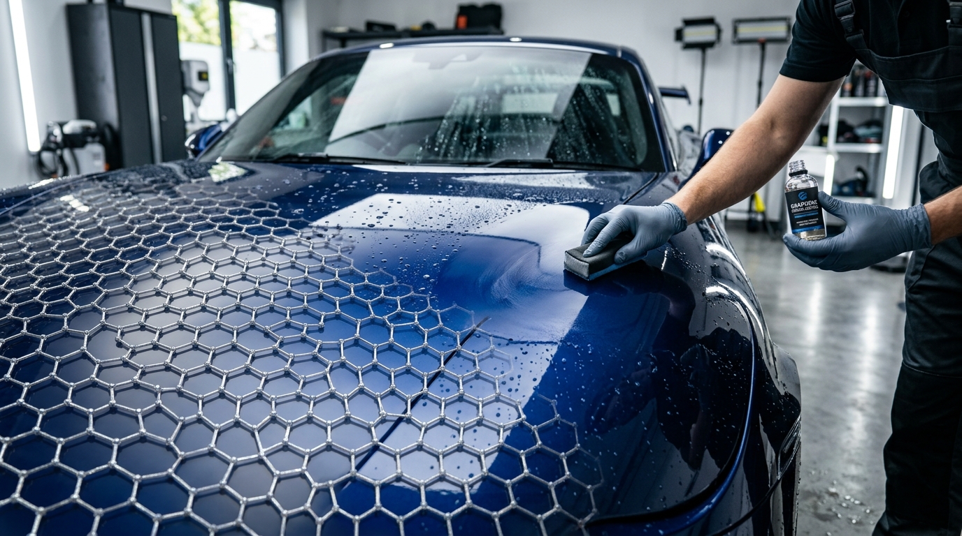
- Corrosion Barriers and Protective Coatings: Graphene’s impermeable hexagonal lattice forms a tortuous barrier that slows the diffusion of oxygen, moisture, and chloride ions toward metal surfaces, extending the lifespan of industrial marine and industrial coatings.
- Lithium-Ion Battery and Supercapacitor Additives: Replacing or augmenting standard carbon black additives with high-conductivity graphene flakes establishes lower-resistance conductive networks within battery cathodes, allowing faster charging rates and improved cyclability.
- Conductive Inks and Flexible Heaters: Printable graphene formulations are deployed in radio-frequency identification (RFID) antennas, automotive de-icing elements, and printed flexible heating circuits.
Emerging Laboratory Frontiers
- Biosensors and Molecular Diagnostics: The extreme surface sensitivity of functionalized graphene field-effect transistors (gFETs) allows label-free detection of single viral particles, nucleic acid sequences, and biochemical markers at ultra-low concentrations.
- Desalination and Separation Membranes: Sub-nanometer pores drilled into monolayer graphene or engineered through laminar GO sheet channels allow selective water permeation while blocking hydrated sodium and chloride ions. Scaling defect-free membrane area remains the primary barrier to adoption.
- Photodetectors and Terahertz Photonics: Ultrafast carrier dynamics enable graphene-based optical modulators and broadband photodetectors that operate across visible, infrared, and terahertz spectral bands.
Engineering Challenges and Material Limitations
Scaling graphene from laboratory synthesis to high-volume manufacturing involves substantial integration hurdles.
Restacking and Agglomeration
Graphene sheets possess immense surface energy and strong inter-sheet van der Waals attraction. In liquid suspensions, composite blends, or dry powders, isolated flakes rapidly agglomerate and re-graphitize, losing their surface area and aspect-ratio advantages unless stabilized by functional groups, surfactants, or matrix-matching compatibilizers.
Interface and Dispersion Engineering
In structural and thermal composites, poor interfacial adhesion between graphene and the host resin creates mechanical weak points and thermal bottlenecks. Surface chemical functionalization improves interfacial bonding and dispersion uniformity, but severe covalent modification disrupts the sp² lattice, reducing intrinsic electrical and mechanical performance.
Quality Verification and Characterization
Assessing commercial graphene shipments requires sophisticated physical characterization. Raman spectroscopy serves as the primary analytical tool to verify layer count, defect levels, and edge structure by analyzing the intensity and shape of the D-band (defect-activated), G-band (sp² in-plane vibration), and 2D-band (second-order overtone). Manufacturers and end-users must also utilize X-ray photoelectron spectroscopy (XPS) for oxygen content, atomic force microscopy (AFM) for flake thickness profiles, and dynamic light scattering (DLS) or scanning electron microscopy (SEM) for lateral flake dimensions.
Frequently Asked Questions
Is graphene completely impermeable to all gases?
A defect-free, single-layer sheet of pristine graphene is impermeable to all standard atoms and gases under ambient conditions, including helium—the smallest atomic gas. Transport occurs only through lattice vacancies, grain boundary tears, or intentionally engineered sub-nanometer pores.
Why has graphene not replaced silicon in computer processors?
Pristine graphene lacks an electronic bandgap, meaning it conducts electricity continuously and cannot be switched off to create the sharp logic states (0 and 1) required for digital computing. While an artificial bandgap can be opened by cutting graphene into narrow nanoribbons or applying mechanical strain, these processes reduce carrier mobility and introduce fabrication defects that eliminate its advantages over silicon.
How is graphene distinguished from graphite?
Graphite consists of millions of stacked graphene layers held together by weak van der Waals forces. While graphite behaves as a bulk anisotropic semi-metal, graphene (specifically 1 to 10 layers) exhibits two-dimensional quantum mechanical behaviors, immense specific surface area, transparency, and mechanical elasticity that disappear in bulk graphite structures.
Is graphene toxic or hazardous to handle?
Graphene nanoplatelets and graphene oxide in dry, respirable powder forms present particulate inhalation risks comparable to other high-aspect-ratio nanomaterials, requiring standard dust collection, HEPA filtration, and personal protective equipment. Once bound within a solid composite, polymer matrix, or liquid slurry, the risk of airborne particle exposure is substantially minimized.